Introduction to pcb printing
Printed circuit boards (PCBs) are essential components in most electronic devices. PCBs provide the foundation to mount and connect electronic components using conductive tracks and pads. As PCBs become more complex with increased component density and more layers, specialized PCB printers have been developed to meet fabrication needs.
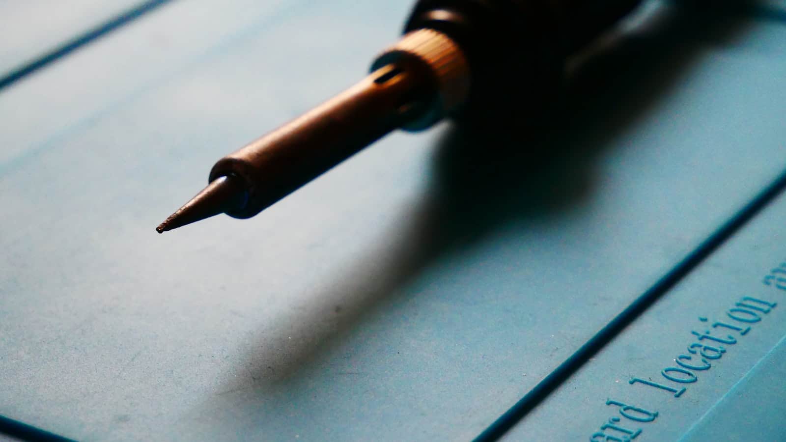
PCB printing refers to using a printer designed specifically for creating printed circuit boards. These printers allow accurate printing of circuit board traces and pads onto the PCB substrate. There are several PCB printing methods available including inkjet printing, aerosol jet printing, screen printing, flexography, gravure printing and more. The printing process deposits conductive inks, which form the conductive tracks, in the desired pattern on the PCB.
Benefits of PCB printing
PCB printing offers several benefits compared to traditional pcb fabrication methods:
- Cost-effective: Printed PCBs can lower prototyping and small-batch production costs
- Fast turnaround: Printed PCBs can be fabricated in just a few hours without the need for costly phototools
- Design flexibility: Printing supports iterative design changes without replenishing phototool inventories
- High resolution: Modern PCB printers support very fine trace geometries and spaces enabling complex board designs
- Simple workflow: Print directly from cad software without manual board layout modifications
PCB printing process overview
The generalized PCB printing process includes:
- Designing circuit board layout files in CAD software
- Converting layouts to printer-compatible file formats
- Preparing and loading PCB substrate materials into printer
- Printing conductive traces using silver, copper or carbon-based inks
- Curing inks by heating to improve conductivity
- Finishing board fabrication with additional printing and plating steps
Actual capabilities and processes vary widely across different PCB printing systems. But in general, these core sub-processes enable practical printed circuit board fabrication.
Conductive inks for PCB printing
Conductive inks enable the deposition of conductive traces onto the insulating PCB substrate. Popular conductive ink materials used in PCB printing include:
- Silver flakes: High conductivity, most common printed PCB ink
- Copper nanoparticles: Lower cost than silver with good conductivity
- Carbon nanotubes and graphene: Lower metal loadings required compared to metal nanoparticle inks
- Conductive polymers: Flexible ink films support flex PCB applications
Inks contain conductive particles like metal flakes/nanoparticles or carbon dispersed in a carrier fluid along with additives. Common carrier fluids and additives include:
- Water-based, soy-based and other eco-friendly carriers
- Organic solvents like terpineol offering faster drying
- Rheology modifiers to optimize ink viscosity
- Binders and adhesion promoters improve substrate sticking
Conductivity Comparison of PCB Printing Inks
| Ink Material | Bulk Resistivity (μΩ cm) | Notes |
|---|---|---|
| Silver Flakes | 1.6 | Best conductivity, high cost |
| Copper Nanoparticles | 2-5 | Lower cost, moderate resistivity |
| Carbon Nanotubes | 50-200 | Lower metal loading, moderate resistivity |
| Conductive Polymers | 0.1-1 kΩ | Flexible films, higher resistivity |
After printing, a curing step typically bakes inks up to peak conductivity by fusing particles together. For silver inks, sintering may further enhance conductivity.

PCB printing methods
There are several printing methods used in fabricating pcb prototypes and production boards. Popular PCB printing approaches include:
Inkjet Printing
Material jetting process deposits precise droplets of conductive inks to build up circuit traces. Two main inkjetting approaches used:
Thermal Inkjet PCB Printing
- Tiny resistive heaters vaporize ink inside print head nozzles
- Vapor bubble forces ink droplet onto substrate
- Low initial system cost, readily available inks
- Slow process with long printing times
Piezoelectric Inkjet Printing
- Uses piezoelectric crystals that change shape when voltage applied
- Rapid pressure pulses force ink droplets out nozzle tips
- Very high print resolution possible
- Faster printing compared to thermal inkjet systems
Aerosol Jet Printing
- Atomizes conductive inks into aerosol droplets in 10-50 micron range
- Focused gas stream directs aerosol mist onto substrate
- Ultra-fine print resolution down to 10 microns
- Builds up traces and pads for conductors up to centimeters thick
- Single-pass printing minimizes alignment errors during multi-layer printing
Screen Printing
- Ink forced through fine mesh screen using squeegee
- Screens define image pattern to be printed
- Deposits thicker ink films compared to other methods
- Widely used for high volume PCB fabrication
- Limited fine feature printing capability
Flexographic Printing
- Raised photopolymer images on printing plate transfer ink patterns
- Fast, high volume roll-to-roll printing process
- 100 nm resolution possible, not as fine as inkjet processes
- Mainly used for high speed printed electronics applications
Printing Process Comparison
| Printing Method | Resolution | Max Aspect Ratio | Build Rate | Notes |
|---|---|---|---|---|
| Thermal Inkjet | 50 μm | 0.05 | Low | Low system cost, slower printing |
| Piezoelectric Inkjet | 1 μm | 0.10 | Medium | Very high resolution printing |
| Aerosol Jet | 10 μm | 1-10 | Medium | Precision printing for 3D structures |
| Screen Printing | 100 μm | 1-10 | High | Widely used process for high volume PCB fabrication |
| Flexographic Printing | 100 nm | 0.05 | Very High | Mainly used in roll-to-roll printed electronics |
PCB substrates
The base pcb material that conductive traces are printed onto is called the substrate. The substrate provides mechanical support and an insulating dielectric layer between conductive layers. Popular substrate options include:
- FR-4 glass epoxy – Most common rigid PCB material
- Polyimide films – Flexible substrates like Kapton for flex PCBs
- Plastic films – PET, PEN, Polycarbonate. Lower temperatures than FR-4
- Paper – Inexpensive substrates with good ink absorption
Since traces are printed directly onto the substrate, it must have properties compatible with the ink and printing process being used. Substrate properties like surface energy, roughness, cure temperature affect print results.
PCB coatings may be applied to the substrate surface before printing to tune the material properties for better ink adhesion and performance. Or additional layers like solder masks can be printed to build up complete circuit boards.
Post-printing PCB processing
For full functionality and reliability, PCBs produced using printing methods often require additional fabrication processing after printing. Common post-printing PCB finishing steps include:
Sintering
Many silver and copper inks requite high temperature sintering after printing:
- Heat treatment fuses metal particles together enhancing conductivity
- Temperatures from 100 – 300°C used depending on metal and substrate
Plating
Plating electrically connects printed conductors and allows soldering:
- Nickel/Immersion Gold: Common finish for solderability
- Electroless Copper: Builds up copper thickness for higher current carrying traces
- Tin: Lower cost but less reliable than Ni/Au finishing
Component Assembly
Printed circuit boards provide the foundation for surface mount device assembly:
- Pick and place machines precisely populate components
- Reflow soldering electrically connects components to board conductors
Conformal Coating
Protective coatings prevent environmental damage during operation:
- Acrylic, silicone, urethane or epoxy coatings shield against moisture, dirt and corrosion
- Selectively printed around components to prevent coating interference
Functional Printing
Additional printing steps create specialized function:
- Embedded passives – Resistors, capacitors integrated directly onto the PCB
- Printed antennas, sensors
- 3D printing builds complex electronics module structures
FAQ
Here are answers to some frequently asked questions about PCB printing:
What materials are used to print circuit boards?
Most PCB printers use specialized conductive inks containing silver, copper or carbon particles suspended in carrier liquids. The metals and carbon provide electrical conductivity when deposited onto the insulating substrate.
Can PCB printing replace traditional PCB fabrication?
For moderate production volumes, PCB printing competes well with processes like chemical etching. Printing supports fast design revisions thanks to no additional phototooling. And additive printing methods avoid the material waste of subtractive fabrication. But traditional high-volume mass production methods like multi-layer silkscreening achieve lower costs through economies of scale.
What printer resolution do I need for PCB fabrication?
Required printing resolution depends on the circuit density and geometry requirements. For simple boards with larger features sizes, lower resolution printers can suffice. But high density interconnects like those with fine pitch quad flat packs require very high resolution printers. Features smaller than 100 micron generally call for specialty processes like inkjet or aerosol jet printing.
Can flexible pcbs be directly printed?
Yes, flexible printed circuit boards on plastic substrates like PET and Kapton can be directly fabricated using PCB printing workflows. Polymer thick film conductive inks designed for flexibility are typically used along with flexible adhesive layers to bond traces to the substrate.
Is heat curing needed for printed PCBs?
Many conductive inks require heat curing to achieve optimal electrical and mechanical properties. Elevated temperatures up to 300°C remove carrier solvents and binders to improve particle contacts. Lower temperature inks are also available for heat sensitive plastics substrates. In these cases, laser or intense pulse light annealing steps may be used instead of traditional thermal ovens.


Leave a Reply