Understanding PCB Warpage
PCB warpage refers to the deviation of a printed circuit board from its intended flat shape. It is a type of deformation where the board bends or curves along one or more axes. The severity of warpage can vary from barely noticeable to severe enough to render the board unusable.
Causes of PCB Warpage
Several factors can contribute to PCB warpage:
-
Thermal Stress: Uneven heating or cooling during the manufacturing process, such as soldering or reflow, can cause thermal stress on the board, leading to warpage.
-
Material Properties: The choice of materials used in the PCB, such as the substrate, copper, and solder mask, can affect its susceptibility to warpage. Different materials have varying coefficients of thermal expansion (CTE), which can result in uneven expansion or contraction.
-
Moisture Absorption: PCBs can absorb moisture from the environment, causing them to expand. If the moisture absorption is uneven across the board, it can lead to warpage.
-
Mechanical Stress: Improper handling, mounting, or packaging of the PCB can introduce mechanical stress, causing the board to warp.
Effects of PCB Warpage
PCB warpage can have several detrimental effects on the functionality and reliability of electronic devices:
-
Assembly Issues: Warped PCBs can be difficult to assemble, as components may not fit properly or make proper contact with the board. This can lead to poor soldering, loose connections, or even component damage.
-
Reduced Reliability: Warped PCBs can cause stress on the components and solder joints, leading to early failure or intermittent issues.
-
Signal Integrity: In high-speed applications, PCB warpage can affect signal integrity by altering the impedance and causing signal reflections or distortions.
-
Mechanical Interference: Severely warped PCBs may not fit properly into the device enclosure or may interfere with other components, causing mechanical issues.
Understanding PCB Twist
PCB twist, also known as board twist or skew, refers to the rotational deformation of a printed circuit board along its longest axis. It occurs when one end of the board is twisted relative to the other end.
Causes of PCB Twist
PCB twist can be caused by various factors:
-
Uneven Copper Distribution: If the copper traces on the PCB are not evenly distributed across the layers, it can cause unbalanced stress, leading to twist.
-
Asymmetric PCB Design: An asymmetric PCB layout, with more components or copper on one side of the board compared to the other, can contribute to twist.
-
Improper Handling: Mishandling of the PCB, such as twisting or bending during assembly or transportation, can introduce twist.
-
Manufacturing Process: Inconsistencies in the manufacturing process, such as uneven pressure during lamination or improper curing of the substrate, can result in PCB twist.
Effects of PCB Twist
PCB twist can have several negative consequences:
-
Assembly Challenges: Twisted PCBs can be difficult to place into the device enclosure or align with other components, leading to assembly issues.
-
Mechanical Stress: Twist can introduce mechanical stress on the PCB, components, and solder joints, potentially causing damage or premature failure.
-
Connectivity Issues: In severe cases, PCB twist can cause disconnection of components or break solder joints, leading to electrical failures.

Preventing PCB Warpage and Twist
To minimize the occurrence of PCB warpage and twist, several preventive measures can be taken during the design and manufacturing stages:
-
Material Selection: Choose PCB materials with similar CTEs to minimize thermal stress. Consider using high-quality, moisture-resistant substrates to reduce warpage due to moisture absorption.
-
Balanced Copper Distribution: Ensure an even distribution of copper traces across the PCB layers to avoid unbalanced stress.
-
Symmetrical PCB Design: Strive for a symmetrical PCB layout, with components and copper evenly distributed on both sides of the board.
-
Thermal Management: Implement proper thermal management techniques, such as using thermal relief pads, to evenly distribute heat during soldering and reflow processes.
-
Controlled Manufacturing Environment: Maintain a controlled manufacturing environment with stable temperature and humidity levels to minimize thermal and moisture-related stresses.
-
Proper Handling and Packaging: Follow proper handling and packaging procedures to avoid mechanical stress on the PCBs during assembly, transportation, and storage.

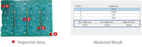
Measuring and Monitoring PCB Warpage and Twist
To ensure the quality and reliability of PCBs, it is essential to measure and monitor warpage and twist throughout the manufacturing process and during the product’s lifecycle.
Measurement Techniques
Several techniques can be used to measure PCB warpage and twist:
-
3D Scanning: 3D scanning technologies, such as laser or optical scanners, can create a detailed 3D model of the PCB, allowing for precise measurement of warpage and twist.
-
Shadow Moiré: Shadow moiré is a non-contact method that uses a grating and a light source to project a shadow pattern onto the PCB surface. The distortion of the shadow pattern indicates the presence of warpage or twist.
-
Coordinate Measuring Machine (CMM): CMMs use a probe to physically touch and measure various points on the PCB surface, providing accurate measurements of warpage and twist.
-
Optical Flatness Measurement: Optical flatness measurement systems use laser or light sensors to measure the deviation of the PCB surface from a reference plane, indicating warpage.
Monitoring and Quality Control
Implementing a robust quality control process is crucial for identifying and addressing PCB warpage and twist issues:
-
Incoming Inspection: Perform incoming inspection of PCBs to identify any warpage or twist issues before assembly.
-
In-Process Monitoring: Monitor the PCBs during the manufacturing process, especially after critical stages such as soldering or reflow, to detect any deformations.
-
Final Inspection: Conduct a thorough final inspection of the assembled PCBs to ensure they meet the specified flatness and twist tolerances.
-
Environmental Testing: Perform environmental testing, such as thermal cycling or humidity exposure, to assess the PCB’s resistance to warpage and twist under various conditions.

FAQ
-
What is the difference between PCB warpage and twist?
PCB warpage refers to the bending or curving of the board along one or more axes, while PCB twist is the rotational deformation of the board along its longest axis. -
Can PCB warpage and twist be completely eliminated?
While it may not be possible to completely eliminate PCB warpage and twist, taking proper preventive measures during the design and manufacturing stages can significantly reduce their occurrence and severity. -
How do I know if my PCB has warpage or twist issues?
Visual inspection, measurements using specialized equipment like 3D scanners or CMMs, and functional testing can help identify PCB warpage and twist issues. -
What are the most common causes of PCB warpage?
The most common causes of PCB warpage include thermal stress, moisture absorption, uneven material properties, and mechanical stress. -
How can I prevent PCB twist in my designs?
To prevent PCB twist, ensure a balanced copper distribution across the layers, strive for a symmetrical PCB layout, and maintain proper handling and manufacturing processes.
Conclusion
PCB warpage and twist are serious issues that can compromise the functionality, reliability, and longevity of electronic devices. Understanding the causes, effects, and prevention methods of these deformations is crucial for designers, manufacturers, and quality control professionals.
By selecting appropriate materials, implementing balanced and symmetrical PCB designs, and following proper manufacturing and handling procedures, the occurrence of PCB warpage and twist can be significantly reduced. Regular monitoring and quality control measures should be in place to identify and address any issues promptly.
Investing in the prevention and management of PCB warpage and twist ultimately leads to higher quality products, improved reliability, and customer satisfaction.


Leave a Reply