Applications of flexible pcbs
Flexible PCBs have some key advantages that make them suitable for certain applications:
Size and Weight
Flexible PCBs can be made very thin and lightweight, occupying less space and adding less weight than a rigid board. This makes them ideal for small, portable electronics.
Dynamic Flexing
The flexible substrate allows the PCB to move, bend, twist and flex dynamically without failing. This is critical in applications like printers and robotics where components need to change positions.
Shape Conforming
Flex circuits can be bent, wrapped or folded to conform to almost any shape. This allows them to fit into tight, curved spaces where a rigid board would not mount properly.
High Density
Components and conductive traces can be placed on both sides of a flex circuit, enabling higher component densities and more efficient layouts than rigid boards.
Some common applications that utilize flexible PCB technology include:
- Wearable electronics
- Medical devices
- Consumer electronics
- Industrial equipment
- Automotive electronics
- Aerospace and military products
Construction and Design
Flexible PCBs have a basic construction consisting of three main elements – the flexible substrate, conductive layers, and stiffeners:
Substrate
The flexible substrate gives the PCB its bendable quality and provides an insulating base. The most common flexible substrate materials are:
- Polyimide (Kapton) – High temperature, chemical resistant
- Polyester (PET) – Lower cost, not as heat tolerant
- PEN – Similar to polyester, but more temperature resistant
Conductors
The conductors are the copper tracks and other conductive materials layered onto the substrate that transmit signals and power between mounted components. Popular conductor options include:
- Rolled annealed copper – Most common, economical option
- Electrolytic copper foil – High conductivity, allows finer trace widths
- Conductive inks – Printed conductors, lower cost
Stiffeners
Since flex circuits are flimsy on their own, stiffeners made of materials like aluminum or FR4 are often added to provide protected mounting areas for components and connectors.
In terms of design, flex PCBs present some unique considerations:
- Trace widths and spacing need to account for flexibility – traces may elongate or crowd as the board moves
- Strain relief cutouts are needed along bend lines to reduce stress
- Careful conductor thickness selection to withstand dynamic flexing
- Minimizing components in flexing sections
Flexible PCB Types
There are several classifications of flex circuits based on their construction and structure:
Single Sided Flexible PCBs
Have conductive traces on only one side of the substrate. Simple and low cost, but lower component density.
Double Sided Flexible PCBs
Have conductive layers on both sides of the substrate. Allows higher component density and more efficient routing while keeping a thin profile.
Multilayer Flexible PCBs
Have three or more conductive layers separated by flexible dielectric material. Allows very complex, high density designs by enabling more interconnection paths.
Rigid-Flex PCBs
Have both rigid and flexible substrates joined together in one circuit board. Combines the benefits of both while providing three-dimensional design capabilities.

flexible pcb manufacturing Process
Producing flexible PCBs requires specialized machinery and techniques tailored to handling thin, bendable materials. Here is an overview of the flex pcb fabrication process:
Substrate Preparation
The raw flexible substrate material such as polyimide or polyester film is unrolled, cut to size, and cleaned. Holes may be punched as part of preparatory steps.
Conductor Application
The conductive material (usually copper foil) is laminated onto the substrate using adhesive and heat pressure rollers. Photoresist may then be applied over the copper.
Imaging
For patterned etching, the circuit layout artwork is directly imaged onto the photoresist using photolithography techniques like laser direct imaging (LDI).
Etching
The board is etched in chemical solutions to remove unwanted copper, leaving only the desired conductive traces protected by the photoresist.
Photoresist Stripping
Once etching is complete, the remaining photoresist is stripped away, resulting in the final conductive pattern on the bare flexible substrate.
Solder Mask & Legend Printing
Solder mask may be applied by laminating or liquid coating, leaving bondable pads exposed. Legend printing adds markings like component IDs and polarity indicators.
Testing & Finishing
Quality assurance testing checks for defects. Stiffeners, cover layers, or encapsulations may be added. The boards are separated and shipped or loaded into assemblies.
Compared to rigid PCB fabrication, specialized flex circuit manufacturing equips include laser direct imagers to shoot artwork directly onto photoresist, vacuum lamination presses, and handling equipment tuned for thin, flexible boards.
Pros and Cons of Flexible PCBs
Flexible PCB technology provides some unique benefits, but also come with tradeoffs to consider depending on the application:
Pros
- Extremely compact and lightweight
- Dynamic flexing capability
- Conforms to three-dimensional shapes
- Allows high component density designs
- Supports rigid-flex board configurations
- Generally faster manufacturing timelines
Cons
- Typically higher cost than rigid PCBs
- Maximum size limitations around 18″ x 24″
- Traces may be more fragile and prone to damage
- Complex design rules and DFM needed
- Advanced manufacturing equipment required
- Limited heat tolerance depending on materials
FQA on Flexible PCBs
What are some key reasons to use a flexible PCB?
Some main reasons to use flex PCB technology are:
- To save space with a very thin, lightweight circuit board
- To support dynamic bending or twisting motion requirements
- To mount onboard non-flat surfaces needing contour matching
- To enable compact, three-dimensional rigid-flex board designs
- To achieve high component density with small components
What are some good applications for flexible circuits?
Typical applications taking advantage of flexible PCB properties include:
- Wearable devices
- Medical instruments like endoscopes
- Industrial robots and motion systems
- Consumer gadgets
- Complex wiring harnesses
- Defense electronics
- Next generation automotive networks
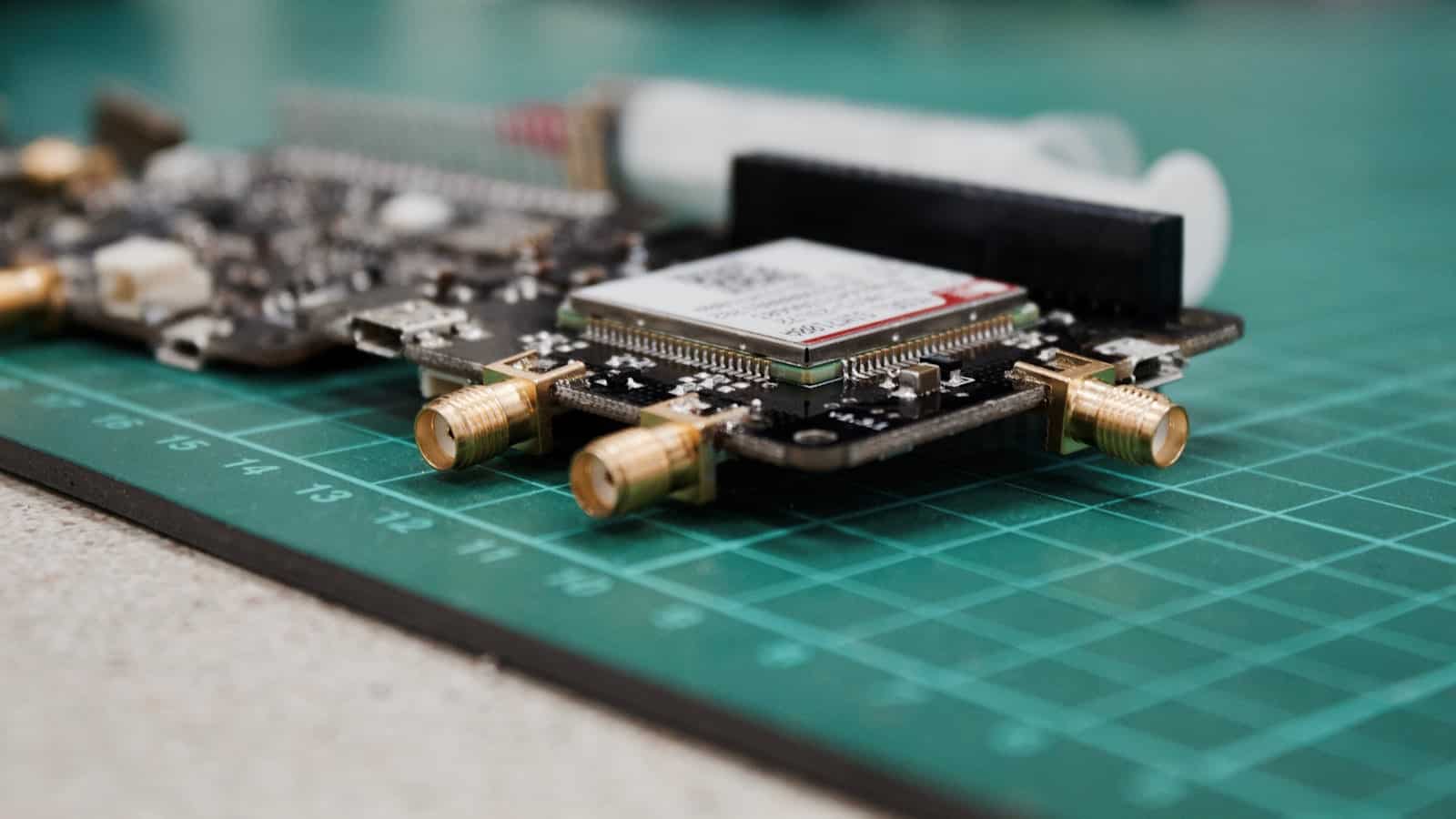
What type of components can be mounted on flex PCBs?
Many conventional surface mount components are compatible with flexible circuit boards, including:
- Resistors and capacitors
- Integrated circuits (ICs)
- Connectors and sockets
- Light emitting diodes (LEDs)
- Chip on board (COB) assemblies
- Sensors, switches and buttons
- crystal oscillators
- Microprocessors
The key is ensuring components are properly adhered and have strain relief in dynamic sections.
Can flex PCBs handle high frequency signals?
Yes, flex circuits can have excellent high frequency signal integrity with tightly controlled impedances, matched lengths, and proper component attachments. Short transmission paths help minimize attenuation at microwave frequencies. Careful layout and shielding helps prevent crosstalk and emi issues.
How much does it cost to have flexible PCBs made?
Cost depends on the flex board complexity, layer count, tolerances, and order quantity. As a rough estimate, simple 2-4 layer flex circuits in small volumes can range from $100 – $500 per square foot, going up to $1,000+ per square foot for complex multilayer designs made domestically in North America.


Leave a Reply