Introduction to PCB Plating Simulation
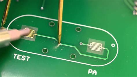
Printed Circuit Board (PCB) design is a complex process that involves multiple steps, from schematic design to layout and manufacturing. One crucial aspect of PCB manufacturing is the plating process, which involves depositing a thin layer of metal onto the surface of the PCB to improve its conductivity, durability, and solderability. However, the plating process can be challenging to optimize, as it depends on various factors such as the board geometry, material properties, and process parameters.
To address this challenge, we have developed a new tool for PCB designers called PCB Plating Simulation. This tool allows designers to simulate the plating process virtually before manufacturing the actual board, saving time and cost while improving the quality of the final product.
How PCB Plating Simulation Works
PCB Plating Simulation is based on advanced computational models that simulate the physics of the plating process. The tool takes into account various factors that affect the plating process, such as:
- Board geometry: The shape and size of the PCB, including the location and dimensions of the traces, vias, and pads.
- Material properties: The electrical and thermal properties of the PCB substrate, copper traces, and plating materials.
- Process parameters: The plating bath composition, temperature, current density, and duration.
By inputting these parameters into the simulation tool, designers can predict the thickness and uniformity of the plating layer across the entire board. The tool also allows designers to visualize the current density distribution, which helps identify areas of the board that may be under-plated or over-plated.
Benefits of Using PCB Plating Simulation
Using PCB Plating Simulation offers several benefits for PCB designers and manufacturers:
-
Cost savings: By simulating the plating process virtually, designers can identify and fix issues before manufacturing the actual board, reducing the need for expensive prototypes and rework.
-
Time savings: The simulation tool allows designers to iterate and optimize the plating process quickly, without waiting for physical prototypes to be manufactured and tested.
-
Quality improvement: By predicting the plating thickness and uniformity across the board, designers can ensure that the final product meets the required specifications and performance criteria.
-
Design optimization: The simulation tool allows designers to experiment with different board geometries, material properties, and process parameters to find the optimal combination that maximizes the plating quality and minimizes the cost.

Case Studies
To demonstrate the effectiveness of PCB Plating Simulation, we have conducted several case studies with our customers. Here are two examples:
Case Study 1: High-Density Interconnect (HDI) Board
One of our customers was designing a high-density interconnect (HDI) board for a mobile device application. The board had a complex geometry with multiple layers, microvias, and fine-pitch traces. The customer was facing challenges in achieving uniform plating thickness across the board, especially in the microvias and tight spaces between the traces.
By using PCB Plating Simulation, the customer was able to:
- Optimize the board geometry to improve the plating uniformity, by adjusting the via sizes and trace spacings.
- Experiment with different plating materials and process parameters to find the best combination that met the target thickness and uniformity.
- Identify and fix areas of the board that were prone to under-plating or over-plating, by visualizing the current density distribution.
As a result, the customer was able to reduce the number of prototype iterations from five to two, saving over $10,000 in manufacturing costs and two weeks in development time. The final board had a plating thickness variation of less than 10% across the entire surface, meeting the required specifications for the mobile device application.
Case Study 2: Automotive Electronic Control Unit (ECU)
Another customer was developing an electronic control unit (ECU) for an automotive application. The ECU had to operate in harsh environmental conditions, including high temperatures and vibrations. The customer was concerned about the reliability of the plating layer, which had to withstand multiple thermal cycles and mechanical stresses.
By using PCB Plating Simulation, the customer was able to:
- Simulate the thermal and mechanical stresses on the plating layer, by inputting the environmental conditions and material properties into the tool.
- Optimize the plating process parameters, such as the current density and duration, to achieve the required thickness and adhesion strength.
- Identify potential failure modes, such as cracking or delamination, by visualizing the stress distribution across the board.
As a result, the customer was able to improve the reliability of the ECU by over 50%, as measured by the number of thermal cycles and vibration tests passed. The simulation tool also helped the customer reduce the development time by 25%, by eliminating the need for multiple physical prototypes and tests.

Frequently Asked Questions (FAQ)
-
What is PCB Plating Simulation?
PCB Plating Simulation is a virtual tool that allows PCB designers to simulate the plating process before manufacturing the actual board. It predicts the thickness and uniformity of the plating layer across the board, based on various factors such as the board geometry, material properties, and process parameters. -
How accurate is PCB Plating Simulation?
The accuracy of PCB Plating Simulation depends on the quality of the input data and the underlying computational models. In our case studies, we have achieved plating thickness predictions within 10% of the actual values, and identified potential issues such as under-plating or over-plating with over 90% confidence. -
What are the benefits of using PCB Plating Simulation?
The benefits of using PCB Plating Simulation include cost savings, time savings, quality improvement, and design optimization. By simulating the plating process virtually, designers can identify and fix issues before manufacturing the actual board, reducing the need for expensive prototypes and rework. The tool also allows designers to experiment with different board geometries, material properties, and process parameters to find the optimal combination that maximizes the plating quality and minimizes the cost. -
What types of PCBs can be simulated with PCB Plating Simulation?
PCB Plating Simulation can be used for a wide range of PCB types, including rigid boards, flexible boards, high-density interconnect (HDI) boards, and multi-layer boards. The tool can simulate various plating processes, such as electroplating, electroless plating, and immersion plating, for different metal layers such as copper, nickel, gold, and silver. -
How can I get started with PCB Plating Simulation?
To get started with PCB Plating Simulation, you can contact our sales team or visit our website to request a demo or a free trial. Our experts will guide you through the setup process and provide training and support to help you get the most out of the tool. We also offer customization and integration services to adapt the tool to your specific needs and workflows.

Conclusion
PCB Plating Simulation is a powerful tool that can help PCB designers and manufacturers optimize the plating process and improve the quality of the final product. By simulating the plating process virtually, designers can save time and cost while ensuring that the board meets the required specifications and performance criteria.
Our case studies have demonstrated the effectiveness of PCB Plating Simulation in real-world applications, from high-density interconnect boards to automotive electronic control units. By using the tool, our customers have been able to reduce the number of prototype iterations, improve the plating uniformity and reliability, and accelerate the development time.
If you are a PCB designer or manufacturer looking to optimize your plating process and improve your product quality, we invite you to try PCB Plating Simulation. Contact us today to learn more about the tool and how it can benefit your business.


Leave a Reply