What is PCB etching?
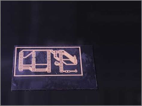
PCB etching is a critical process in the production of printed circuit boards (PCBs) where unwanted copper is removed from the laminate surface to create the desired circuit pattern. The etching process selectively removes copper from areas not protected by the etch resist, leaving behind the intended conductive traces, pads, and vias that form the functional circuitry on the PCB.
Types of PCB Etching
There are two primary methods used for PCB etching:
-
Wet Etching: This method involves submerging the PCB in a chemical solution (etchant) that dissolves the unprotected copper. Common etchants used in wet etching include ferric chloride, ammonium persulfate, and cupric chloride.
-
Dry Etching: In this method, a plasma or gas is used to remove the unwanted copper. Dry etching is less common in PCB production compared to wet etching due to higher equipment costs and complexity.
The Inner Layer Etching Process
In multi-layer PCBs, the inner layers are etched before they are laminated together with the outer layers and prepreg. The inner layer etching process typically follows these steps:
1. Cleaning and Surface Preparation
Before etching, the inner layer copper surface is cleaned to remove any contaminants, such as dirt, grease, or oxidation. This ensures proper adhesion of the photoresist and consistent etching results. Common cleaning methods include:
- Chemical cleaning using alkaline or acid solutions
- Mechanical cleaning using brushes or abrasives
- Plasma cleaning to remove organic contaminants
2. Applying Photoresist
A photoresist is a light-sensitive polymer that is applied to the copper surface to create the desired circuit pattern. There are two types of photoresists:
- Dry film photoresist (DFR): A solid film that is laminated onto the copper surface using heat and pressure.
- Liquid photoresist (LPI): A liquid that is spin-coated or sprayed onto the copper surface and then dried.
The choice of photoresist depends on factors such as the desired feature size, resolution, and production volume.
3. Exposing and Developing the Photoresist
Once the photoresist is applied, it is exposed to UV light through a photomask or phototool. The photomask contains the desired circuit pattern and selectively blocks UV light from reaching certain areas of the photoresist.
For negative photoresists, the exposed areas become insoluble in the developer solution, while unexposed areas remain soluble. For positive photoresists, the opposite occurs—exposed areas become soluble, while unexposed areas remain insoluble.
After exposure, the photoresist is developed using a chemical solution that removes the soluble areas, revealing the underlying copper that will be etched away.
4. Etching the Copper
The inner layer panel is then submerged in the etching solution, which chemically removes the copper not protected by the developed photoresist. The etching process is carefully controlled to ensure consistent results and minimize undercut (lateral etching beneath the photoresist).
Factors that influence the etching process include:
- Etchant composition and concentration
- Temperature
- Agitation
- Etch time
After etching, the panel is rinsed to remove any remaining etchant and byproducts.
5. Stripping the Photoresist
After etching, the remaining photoresist is removed using a chemical stripper or a combination of chemical and mechanical methods. This reveals the final etched copper pattern on the inner layer.
6. Inspection and Quality Control
The etched inner layer undergoes visual and automated optical inspection (AOI) to ensure that the circuit pattern meets the design specifications and is free of defects, such as:
- Open circuits
- Short circuits
- Overetching or underetching
- Contamination
Electrical testing may also be performed to verify the continuity and isolation of the circuits.

Challenges in Inner Layer Etching
Several challenges can arise during the inner layer etching process that can impact the quality and reliability of the final PCB:
1. Etchant Management
Proper management of the etching solution is crucial for consistent results. Factors to consider include:
- Etchant concentration: Over time, the etchant becomes depleted and must be replenished or replaced to maintain consistent etching rates.
- Etchant contamination: Copper and other byproducts can accumulate in the etchant, affecting its performance. Filtration and chemical treatment can help maintain etchant quality.
- Temperature control: Etching rates are temperature-dependent, so consistent temperature control is essential for predictable results.
2. Undercut and Overetching
Undercut occurs when the etchant removes copper beneath the photoresist, resulting in narrower traces than intended. Overetching occurs when the etchant removes too much copper, causing traces to become too thin or even disappear entirely. Factors that contribute to undercut and overetching include:
- Etchant concentration and temperature
- Etching time
- Photoresist adhesion and durability
- Feature size and spacing
Careful process control and optimization can help minimize undercut and overetching.
3. Photoresist Adhesion and Resolution
Proper photoresist adhesion is critical for achieving clean, well-defined etched features. Poor adhesion can lead to etchant penetration beneath the photoresist, causing undercut or loss of features. Factors that affect photoresist adhesion include:
- Surface cleanliness and preparation
- Photoresist application and drying conditions
- Exposure and development parameters
High-resolution features require the use of advanced photoresists and imaging technologies, such as direct imaging (DI) or laser direct imaging (LDI), to achieve the necessary precision and accuracy.
4. Etch Factor and Aspect Ratio
The etch factor is the ratio of the etch depth to the undercut. A higher etch factor indicates more vertical sidewalls and less undercut. The aspect ratio is the ratio of the feature depth to its width. High aspect ratios can be challenging to etch consistently due to differences in etchant accessibility and depletion rates.
Optimizing the etching process for high etch factors and aspect ratios may involve adjusting etchant composition, temperature, and agitation, as well as using advanced photoresists and imaging techniques.

Advancements in Inner Layer Etching
Recent advancements in inner layer etching technology have focused on improving precision, efficiency, and environmental sustainability:
1. Direct Imaging (DI) and Laser Direct Imaging (LDI)
DI and LDI systems use high-resolution digital imaging to directly expose the photoresist, eliminating the need for traditional photomasks. This allows for faster turnaround times, improved feature resolution, and greater flexibility in design changes.
2. Inkjet Etch Resist
Inkjet printing technology can be used to directly apply etch resist to the copper surface, creating the desired circuit pattern without the need for photoresist and exposure. This process offers advantages such as reduced material waste, faster turnaround times, and the ability to easily customize designs.
3. Environmentally Friendly Etchants
Traditional etchants, such as ferric chloride, can pose environmental and health risks due to their toxicity and disposal requirements. Newer, more environmentally friendly etchants, such as acidified cupric chloride and alkaline etchants, have been developed to reduce the environmental impact of PCB etching.
4. Vertical Continuous Etching (VCE)
VCE is a continuous etching process that uses a vertically oriented conveyor system to transport panels through the etching solution. This method offers improved efficiency, consistency, and etchant management compared to traditional batch etching processes.

Frequently Asked Questions (FAQ)
1. What is the difference between inner layer and outer layer etching?
Inner layer etching is performed on the internal layers of a multi-layer PCB before they are laminated together with the outer layers and prepreg. Outer layer etching is performed on the top and bottom layers of the PCB after lamination. The main difference is that inner layer etching requires more precise alignment and registration to ensure proper layer-to-layer connectivity.
2. What are the most common etchants used in PCB inner layer etching?
The most common etchants used in PCB inner layer etching are ferric chloride (FeCl3), ammonium persulfate ((NH4)2S2O8), and cupric chloride (CuCl2). Each etchant has its advantages and disadvantages in terms of etching speed, selectivity, and environmental impact.
3. How does the etching process affect the signal integrity of a PCB?
The etching process can affect signal integrity by influencing factors such as trace width, thickness, and roughness. Overetching can cause traces to become too thin or discontinuous, leading to increased resistance and potential signal loss. Underetching can result in traces that are too wide, which may cause impedance mismatches and signal reflections. Proper control of the etching process is essential for maintaining the desired trace geometry and minimizing signal integrity issues.
4. What role does the etch factor play in inner layer etching?
The etch factor is the ratio of the etch depth to the undercut. A higher etch factor indicates more vertical sidewalls and less undercut, which is desirable for achieving precise feature geometries and minimizing signal integrity issues. Optimizing the etch factor involves careful control of etchant composition, temperature, and agitation, as well as the use of high-quality photoresists and imaging techniques.
5. How can the environmental impact of PCB etching be reduced?
Several strategies can be employed to reduce the environmental impact of PCB etching:
- Using more environmentally friendly etchants, such as acidified cupric chloride or alkaline etchants, instead of traditional ferric chloride.
- Implementing closed-loop etching systems that recycle and reuse etchant solutions.
- Employing direct imaging or inkjet etch resist technologies to reduce material waste and energy consumption.
- Proper treatment and disposal of etching byproducts and waste streams in accordance with local regulations.
By adopting these measures, PCB manufacturers can minimize the environmental footprint of the etching process while still achieving high-quality results.
Conclusion
Etching inner layers is a critical step in the production of multi-layer PCBs, as it creates the conductive pathways that form the foundation of the circuit. The process involves selectively removing unwanted copper from the laminate surface using chemical etchants, leaving behind the desired circuit pattern defined by the photoresist.
Proper control of the etching process, including etchant management, photoresist application, and exposure and development parameters, is essential for achieving precise, reliable results. Challenges such as undercut, overetching, and photoresist adhesion must be addressed through careful process optimization and the use of advanced technologies.
Recent advancements in inner layer etching, such as direct imaging, inkjet etch resist, and environmentally friendly etchants, have helped improve the precision, efficiency, and sustainability of the process. As PCB designs continue to push the boundaries of miniaturization and performance, innovation in inner layer etching will remain crucial for meeting the evolving demands of the electronics industry.


Leave a Reply