Why is PCB X-ray Inspection Important?
PCB X-ray inspection is crucial for several reasons:
-
Detecting hidden defects: X-ray inspection can reveal defects that are not visible to the naked eye or other inspection methods, such as optical inspection.
-
Ensuring product quality: By identifying and addressing defects early in the manufacturing process, X-ray inspection helps maintain the quality of the final product.
-
Saving time and money: Detecting defects early can prevent costly rework or product failures in the field, ultimately saving time and money for the manufacturer.
-
Meeting industry standards: Many industries, such as aerospace and medical devices, require stringent quality control measures, including X-ray inspection, to ensure the reliability and safety of their products.
How Does PCB X-ray Inspection Work?
PCB X-ray inspection works by passing X-rays through the PCB and creating a digital image based on the absorption of the X-rays by the different materials in the board. The basic components of an X-ray inspection system include:
- X-ray source: Generates the X-rays that penetrate the PCB.
- X-ray detector: Captures the X-rays that pass through the PCB and converts them into a digital image.
- Image processing software: Analyzes the digital image to identify defects and anomalies.
The X-ray inspection process typically involves the following steps:
- Placing the PCB in the inspection system.
- Generating X-rays and directing them through the PCB.
- Capturing the X-rays that pass through the PCB with the detector.
- Creating a digital image of the PCB’s internal structure.
- Analyzing the image using specialized software to identify defects and anomalies.

Types of PCB X-ray Inspection Systems
There are two main types of PCB X-ray inspection systems:
-
2D X-ray Inspection: This method provides a two-dimensional view of the PCB, allowing for the detection of defects such as broken traces, short circuits, and missing components. 2D X-ray inspection is faster and more cost-effective than 3D inspection but may not detect all types of defects.
-
3D X-ray Inspection: Also known as computed tomography (CT) inspection, this method creates a three-dimensional image of the PCB by combining multiple 2D images taken from different angles. 3D X-ray inspection can detect more complex defects, such as voids in solder joints, but is slower and more expensive than 2D inspection.
| Inspection Type | Advantages | Disadvantages |
|---|---|---|
| 2D X-ray | – Faster inspection speed – Lower cost |
– May not detect all defect types |
| 3D X-ray (CT) | – Detects more complex defects – Provides a 3D view of the PCB |
– Slower inspection speed – Higher cost |

Common Defects Detected by PCB X-ray Inspection
PCB X-ray inspection can detect a wide range of defects, including:
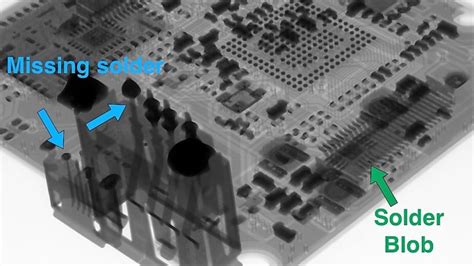
- Solder joint defects: Voids, cracks, bridges, and insufficient or excessive solder.
- Component defects: Missing, misaligned, or damaged components.
- PCB substrate defects: Delamination, cracks, and voids in the PCB substrate.
- Trace defects: Broken, shorted, or narrowed traces.
- Barrel fill defects: Insufficient or excessive plating in through-holes and vias.

Advantages of PCB X-ray Inspection
PCB X-ray inspection offers several advantages over other inspection methods:
- Non-destructive testing: X-ray inspection does not damage the PCB, allowing for 100% inspection of production units.
- Detection of hidden defects: X-ray inspection can reveal defects that are not visible to the naked eye or other inspection methods.
- Inspection of complex assemblies: X-ray inspection can be used to inspect complex PCB assemblies, such as multi-layer boards and high-density interconnect (HDI) designs.
- Automated inspection: X-ray inspection systems can be automated, allowing for faster and more consistent inspection results.
Limitations of PCB X-ray Inspection
Despite its many advantages, PCB X-ray inspection has some limitations:
- Cost: X-ray inspection systems can be expensive, especially for smaller manufacturers.
- Radiation safety: X-ray inspection systems emit ionizing radiation, which requires proper safety measures and training for operators.
- Limited material detection: Some materials, such as plastics and organic compounds, may not be easily detected by X-ray inspection.
- False positives and negatives: X-ray inspection systems may occasionally generate false positive or false negative results, requiring additional verification.
Implementing PCB X-ray Inspection in the Manufacturing Process
To effectively implement PCB X-ray inspection in the manufacturing process, consider the following steps:
- Determine inspection requirements: Identify the types of defects that need to be detected and the required inspection coverage.
- Select the appropriate inspection system: Choose between 2D and 3D X-ray inspection systems based on the complexity of the PCB designs and the types of defects to be detected.
- Develop inspection protocols: Establish standard operating procedures for X-ray inspection, including sample selection, system settings, and image analysis criteria.
- Train personnel: Ensure that operators are properly trained in the use of the X-ray inspection system and the interpretation of inspection results.
- Integrate with other quality control measures: Use X-ray inspection in conjunction with other quality control methods, such as optical inspection and electrical testing, to ensure comprehensive defect detection.
Frequently Asked Questions (FAQ)
- Is X-ray inspection safe for PCBs?
Yes, X-ray inspection is a non-destructive testing method that does not damage the PCB or its components. However, proper safety measures must be in place to protect operators from radiation exposure.
- Can X-ray inspection detect all types of PCB defects?
While X-ray inspection is a powerful tool for detecting many types of defects, it may not be able to detect all defects, particularly those related to certain materials or surface-level anomalies. It is often used in combination with other inspection methods to ensure comprehensive defect detection.
- How long does X-ray inspection take?
The duration of X-ray inspection depends on factors such as the complexity of the PCB, the type of inspection system (2D or 3D), and the number of boards being inspected. 2D inspection is generally faster than 3D inspection, but the exact time can vary from a few seconds to several minutes per board.
- Is X-ray inspection required for all PCBs?
While X-ray inspection is not required for all PCBs, it is often necessary for high-reliability applications, such as aerospace, medical devices, and automotive electronics. Some industry standards and regulations may also mandate the use of X-ray inspection for certain products.
- How much does an X-ray inspection system cost?
The cost of an X-ray inspection system can vary widely depending on factors such as the type of system (2D or 3D), the level of automation, and the manufacturer. Entry-level 2D systems may cost tens of thousands of dollars, while high-end 3D systems can cost hundreds of thousands or even millions of dollars. However, the cost of an X-ray inspection system should be weighed against the potential savings in terms of improved product quality and reduced warranty claims.
Conclusion
PCB X-ray inspection is a powerful and essential tool for ensuring the quality and reliability of printed circuit boards. By allowing manufacturers to detect hidden defects and anomalies, X-ray inspection helps to prevent costly rework and product failures in the field. As PCB designs become increasingly complex and miniaturized, the importance of X-ray inspection in the manufacturing process will only continue to grow. By implementing X-ray inspection in conjunction with other quality control measures, manufacturers can improve product quality, reduce costs, and meet the demanding requirements of today’s electronics industry.


Leave a Reply