What are PCB Outlines?
PCB outlines, also known as PCB board outlines or PCB contours, refer to the physical shape and dimensions of a printed circuit board (PCB). The outline defines the external boundaries of the PCB and includes any cutouts, notches, or special features required for the board’s intended application. Defining the correct PCB outline is crucial for ensuring proper fit and functionality within the device or system in which the PCB will be installed.
Types of PCB Outlines
There are several common types of PCB outlines, each with its own characteristics and applications:
-
Rectangular: The most basic and widely used PCB outline, rectangular boards are simple to design and manufacture. They are suitable for a wide range of applications and are easy to fit into standard enclosures.
-
Circular: Circular PCBs are often used in applications where space is limited or a specific form factor is required, such as in wearable devices or circular connectors.
-
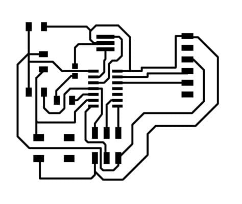
Irregular: Irregular PCB outlines are custom-designed to fit specific enclosures or to accommodate unique component placements. These outlines may include cutouts, notches, or curved edges to ensure optimal space utilization and compatibility with the intended device.
Factors to Consider When Designing PCB Outlines
When designing a PCB outline, several factors must be taken into account to ensure optimal performance and manufacturability:
-
Enclosure compatibility: The PCB outline must be designed to fit perfectly within the intended enclosure or device. This requires close collaboration between the PCB designer and the mechanical engineer responsible for the enclosure design.
-
Component placement: The outline should accommodate the placement of all necessary components, including connectors, mounting holes, and any special features such as heatsinks or shielding.
-
Manufacturing constraints: The PCB outline must adhere to the manufacturing capabilities of the chosen PCB fabricator. This includes minimum feature sizes, tolerances, and any specific design rules related to the fabrication process.
-
Assembly requirements: The outline should facilitate easy assembly of the PCB into the final device, considering factors such as connector orientation, mounting hole locations, and accessibility for automated assembly processes.
PCB Outline Design Process
The PCB outline design process typically involves the following steps:
-
Define requirements: Gather information about the intended application, enclosure dimensions, and any specific features or constraints that will impact the PCB outline.
-
Create initial outline: Using PCB design software, create an initial outline based on the requirements. This may involve importing CAD files of the enclosure or creating the outline from scratch.
-
Place components: Arrange the necessary components on the PCB, ensuring proper placement and orientation relative to the outline.
-
Refine outline: Adjust the outline as needed to accommodate component placement, mounting holes, and any other required features.
-
Verify manufacturability: Check the PCB outline against the fabricator’s design rules and constraints to ensure it can be manufactured reliably and cost-effectively.
-
Collaborate with mechanical engineer: Work closely with the mechanical engineer to ensure the PCB outline is compatible with the enclosure design and assembly process.
-
Finalize and document: Once the outline is finalized, create detailed documentation, including dimensioned drawings and any necessary fabrication notes.

Best Practices for PCB Outline Design
To ensure a successful PCB outline design, consider the following best practices:
-
Keep it simple: Whenever possible, use simple, straightforward outlines to minimize manufacturing complexity and cost.
-
Plan for assembly: Consider the assembly process when designing the outline, ensuring that components are accessible and the board can be easily integrated into the final device.
-
Allow for tolerances: Include appropriate tolerances in the outline design to account for manufacturing variability and ensure proper fit within the enclosure.
-
Communicate clearly: Maintain clear communication with the mechanical engineer and PCB fabricator throughout the design process to avoid misunderstandings and ensure a seamless integration of the PCB into the final product.
-
Test and prototype: Before finalizing the design, create prototypes and test the PCB outline for fit and functionality within the intended enclosure.

Common PCB Outline Design Challenges and Solutions
Designers may encounter various challenges when creating PCB outlines. Some common issues and their solutions include:
-
Limited space: When working with tight space constraints, consider using smaller components, optimizing component placement, or exploring alternative packaging options, such as chip-scale packages or bare die.
-
Complex shapes: For irregular or complex outlines, use PCB design software with advanced shape-creation tools and work closely with the fabricator to ensure manufacturability.
-
High-density designs: In high-density PCB designs, pay close attention to component placement and routing to avoid conflicts with the outline and ensure adequate clearances.
-
Thermal management: If the PCB generates significant heat, incorporate features such as heatsinks or thermal vias into the outline design to facilitate effective heat dissipation.
-
Mechanical stress: For applications subject to high mechanical stress, reinforce the PCB outline with additional mounting points or support structures to minimize the risk of damage.

PCB Outline Design Tools and Resources
Several PCB design software packages offer tools and resources for creating and optimizing PCB outlines. Some popular options include:
-
Altium Designer: A comprehensive PCB design suite with advanced outline creation and editing tools.
-
KiCad: A free, open-source PCB design software with a robust set of outline design features.
-
Eagle: A widely-used PCB design software with intuitive outline creation tools and an extensive library of pre-designed outlines.
-
Cadence OrCAD: A powerful PCB design platform with advanced outline design capabilities and integration with mechanical CAD tools.
In addition to these software tools, numerous online resources, such as forums, tutorials, and design guides, can help designers create effective PCB outlines.
FAQ
-
What is the importance of a well-designed PCB outline?
A well-designed PCB outline ensures proper fit and functionality within the intended device or enclosure, facilitates efficient manufacturing and assembly, and minimizes the risk of mechanical or thermal issues. -
How can I ensure my PCB outline is manufacturable?
To ensure manufacturability, work closely with your PCB fabricator, adhere to their design rules and constraints, and incorporate appropriate tolerances into your outline design. -
What should I do if my PCB outline is too complex for standard manufacturing processes?
If your PCB outline is too complex, consider simplifying the design, exploring alternative manufacturing processes, or working with a fabricator specializing in complex or custom PCB designs. -
How can I optimize my PCB outline for thermal management?
To optimize your PCB outline for thermal management, incorporate features such as heatsinks, thermal vias, or cooling channels, and ensure adequate airflow around the board. -
What are the benefits of using pre-designed PCB outlines?
Using pre-designed PCB outlines can save time and effort in the design process, ensure compatibility with standard enclosures or components, and minimize the risk of design errors or manufacturability issues.
| PCB Outline Type | Advantages | Disadvantages |
|---|---|---|
| Rectangular | – Simple to design and manufacture – Widely compatible with standard enclosures and components |
– May not be optimal for space-constrained or unique applications |
| Circular | – Suitable for space-constrained or circular enclosures – Can provide a unique aesthetic appeal |
– Limited component placement options – May require specialized manufacturing processes |
| Irregular | – Allows for custom fit within unique enclosures – Facilitates optimal space utilization |
– Increased design complexity – Higher manufacturing costs and lead times |
In conclusion, a well-designed PCB outline is essential for ensuring the proper fit, functionality, and manufacturability of a printed circuit board. By considering factors such as enclosure compatibility, component placement, manufacturing constraints, and assembly requirements, and following best practices and collaborating closely with mechanical engineers and fabricators, designers can create PCB outlines that meet the unique needs of their applications while minimizing costs and time-to-market.


Leave a Reply