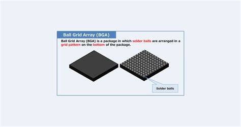
Plastic BGA (PBGA)
The Plastic Ball Grid Array (PBGA) is the most common type of BGA package. It uses a plastic substrate and is suitable for a wide range of applications. The PBGA package offers several advantages, including:
- Lower cost compared to ceramic BGA packages
- Good thermal and electrical performance
- Available in various sizes and pin counts
- Suitable for high-volume production
| Characteristic | Description |
|---|---|
| Substrate Material | BT Resin, FR-4 |
| Thermal Conductivity | 0.3 – 0.5 W/mK |
| CTE | 15 – 18 ppm/°C |
| Moisture Sensitivity Level (MSL) | 2a – 3 |
| Package Thickness | 1.0 – 2.5 mm |
| Pitch | 0.8 – 1.27 mm |
Common PBGA Package Sizes
| Package Size | Pin Count Range | Body Size (mm) | Pitch (mm) |
|---|---|---|---|
| PBGA-119 | 119 – 132 | 8 x 8 | 0.8 |
| PBGA-225 | 225 – 256 | 15 x 15 | 1.0 |
| PBGA-324 | 324 – 361 | 17 x 17 | 1.0 |
| PBGA-400 | 400 – 484 | 21 x 21 | 1.0 |
| PBGA-625 | 625 – 676 | 27 x 27 | 1.0 |
Ceramic BGA (CBGA)
Ceramic Ball Grid Array (CBGA) packages use a ceramic substrate, which offers better thermal and electrical performance compared to plastic BGA packages. CBGAs are suitable for high-performance applications that require better heat dissipation and reliability. Key features of CBGA packages include:
- Higher thermal conductivity compared to PBGA
- Lower CTE, providing better thermal cycling performance
- Higher cost compared to PBGA
- Suitable for high-reliability applications
| Characteristic | Description |
|---|---|
| Substrate Material | Alumina (Al2O3), Aluminum Nitride (AlN) |
| Thermal Conductivity | 20 – 180 W/mK |
| CTE | 6 – 8 ppm/°C |
| Moisture Sensitivity Level (MSL) | 1 |
| Package Thickness | 1.0 – 2.5 mm |
| Pitch | 1.0 – 1.27 mm |
Common CBGA Package Sizes
| Package Size | Pin Count Range | Body Size (mm) | Pitch (mm) |
|---|---|---|---|
| CBGA-256 | 256 – 324 | 17 x 17 | 1.0 |
| CBGA-432 | 432 – 480 | 21 x 21 | 1.0 |
| CBGA-625 | 625 – 676 | 27 x 27 | 1.0 |
| CBGA-1152 | 1152 – 1296 | 35 x 35 | 1.0 |

Fine-Pitch BGA (FBGA)
Fine-Pitch Ball Grid Array (FBGA) packages offer a smaller pitch (distance between solder balls) compared to standard BGA packages. FBGAs are suitable for high-density applications that require a large number of interconnections in a small package size. Key features of FBGA packages include:
- Pitch size ranging from 0.4 mm to 0.8 mm
- Higher pin count density compared to standard BGA packages
- Available in both plastic and ceramic substrates
- Suitable for high-density, high-performance applications
| Characteristic | Description |
|---|---|
| Substrate Material | BT Resin, FR-4, Alumina (Al2O3), Aluminum Nitride (AlN) |
| Thermal Conductivity | 0.3 – 180 W/mK |
| CTE | 6 – 18 ppm/°C |
| Moisture Sensitivity Level (MSL) | 1 – 3 |
| Package Thickness | 0.5 – 1.5 mm |
| Pitch | 0.4 – 0.8 mm |
Common FBGA Package Sizes
| Package Size | Pin Count Range | Body Size (mm) | Pitch (mm) |
|---|---|---|---|
| FBGA-256 | 256 – 324 | 10 x 10 | 0.8 |
| FBGA-484 | 484 – 576 | 15 x 15 | 0.8 |
| FBGA-676 | 676 – 900 | 17 x 17 | 0.8 |
| FBGA-1156 | 1156 – 1369 | 23 x 23 | 0.8 |

Tape BGA (TBGA)
Tape Ball Grid Array (TBGA) packages use a thin, flexible tape substrate instead of the traditional rigid substrates used in PBGA and CBGA packages. TBGAs offer several advantages, including:
- Thinner package profile compared to PBGA and CBGA
- Flexibility, allowing for better stress absorption during thermal cycling
- Lower cost compared to ceramic BGA packages
- Suitable for applications requiring a thin, lightweight package
| Characteristic | Description |
|---|---|
| Substrate Material | Polyimide |
| Thermal Conductivity | 0.2 – 0.3 W/mK |
| CTE | 15 – 20 ppm/°C |
| Moisture Sensitivity Level (MSL) | 2a – 3 |
| Package Thickness | 0.5 – 1.0 mm |
| Pitch | 0.5 – 0.8 mm |
Common TBGA Package Sizes
| Package Size | Pin Count Range | Body Size (mm) | Pitch (mm) |
|---|---|---|---|
| TBGA-64 | 64 – 100 | 5 x 5 | 0.5 |
| TBGA-196 | 196 – 256 | 10 x 10 | 0.65 |
| TBGA-324 | 324 – 400 | 13 x 13 | 0.65 |
| TBGA-484 | 484 – 576 | 15 x 15 | 0.65 |

Chip-Scale BGA (CSBGA)
Chip-Scale Ball Grid Array (CSBGA) packages are designed to have a package size similar to the die size, with a package size no more than 1.2 times the die size. CSBGAs offer a high-density, compact solution for applications with limited board space. Key features of CSBGA packages include:
- Package size similar to the die size
- Very thin profile, typically less than 1.0 mm
- High-density interconnections
- Suitable for applications with limited board space
| Characteristic | Description |
|---|---|
| Substrate Material | BT Resin, FR-4 |
| Thermal Conductivity | 0.3 – 0.5 W/mK |
| CTE | 15 – 18 ppm/°C |
| Moisture Sensitivity Level (MSL) | 2a – 3 |
| Package Thickness | 0.5 – 1.0 mm |
| Pitch | 0.4 – 0.8 mm |
Common CSBGA Package Sizes
| Package Size | Pin Count Range | Body Size (mm) | Pitch (mm) |
|---|---|---|---|
| CSBGA-64 | 64 – 100 | 3 x 3 | 0.5 |
| CSBGA-144 | 144 – 196 | 6 x 6 | 0.5 |
| CSBGA-256 | 256 – 324 | 8 x 8 | 0.5 |
| CSBGA-400 | 400 – 484 | 10 x 10 | 0.5 |
Stacked-Die BGA (SDBGA)
Stacked-Die Ball Grid Array (SDBGA) packages incorporate multiple dies stacked vertically within a single package. SDBGAs offer increased functionality and performance in a compact package size. Key features of SDBGA packages include:
- Multiple dies stacked vertically
- Increased functionality and performance
- Reduced package size compared to using multiple single-die packages
- Available in both plastic and ceramic substrates
| Characteristic | Description |
|---|---|
| Substrate Material | BT Resin, FR-4, Alumina (Al2O3), Aluminum Nitride (AlN) |
| Thermal Conductivity | 0.3 – 180 W/mK |
| CTE | 6 – 18 ppm/°C |
| Moisture Sensitivity Level (MSL) | 2a – 3 |
| Package Thickness | 1.0 – 2.5 mm |
| Pitch | 0.65 – 1.27 mm |
Common SDBGA Package Configurations
| Configuration | Description |
|---|---|
| 2-Die Stack | Two dies stacked vertically |
| 4-Die Stack | Four dies stacked vertically |
| 8-Die Stack | Eight dies stacked vertically |
| Mixed-Die Stack | Different die types or sizes stacked vertically |
System-in-Package BGA (SiPBGA)
System-in-Package Ball Grid Array (SiPBGA) packages integrate multiple dies and passive components into a single package, creating a complete system or subsystem. SiPBGAs offer a highly integrated, compact solution for complex applications. Key features of SiPBGA packages include:
- Integration of multiple dies and passive components
- Highly integrated system or subsystem in a single package
- Reduced board space and simplified board design
- Available in both plastic and ceramic substrates
| Characteristic | Description |
|---|---|
| Substrate Material | BT Resin, FR-4, Alumina (Al2O3), Aluminum Nitride (AlN) |
| Thermal Conductivity | 0.3 – 180 W/mK |
| CTE | 6 – 18 ppm/°C |
| Moisture Sensitivity Level (MSL) | 2a – 3 |
| Package Thickness | 1.0 – 3.0 mm |
| Pitch | 0.65 – 1.27 mm |
Common SiPBGA Package Configurations
| Configuration | Description |
|---|---|
| Multi-Chip Module (MCM) | Multiple dies interconnected on a single substrate |
| Package-on-Package (PoP) | Stacking of multiple BGA packages |
| 2.5D Integration | Dies interconnected using an interposer |
| 3D Integration | Dies stacked and interconnected using through-silicon vias (TSVs) |
Frequently Asked Questions (FAQ)
- Q: What is the main difference between plastic and ceramic BGA packages?
A: The main difference between plastic and ceramic BGA packages is the substrate material. Plastic BGA (PBGA) packages use a plastic substrate, typically BT resin or FR-4, while ceramic BGA (CBGA) packages use a ceramic substrate, such as alumina or aluminum nitride. Ceramic substrates offer better thermal conductivity and lower CTE compared to plastic substrates, making them suitable for high-performance, high-reliability applications. However, ceramic packages are generally more expensive than plastic packages. - Q: What is the advantage of using a fine-pitch BGA (FBGA) package?
A: The main advantage of using a fine-pitch BGA (FBGA) package is the increased pin count density compared to standard BGA packages. FBGAs have a smaller pitch (distance between solder balls), typically ranging from 0.4 mm to 0.8 mm, allowing for more interconnections in a smaller package size. This makes FBGAs suitable for high-density, high-performance applications where board space is limited. - Q: What are the benefits of using a tape BGA (TBGA) package?
A: Tape BGA (TBGA) packages offer several benefits, including a thinner package profile, flexibility, and lower cost compared to ceramic BGA packages. The thin, flexible tape substrate used in TBGAs allows for better stress absorption during thermal cycling, improving package reliability. Additionally, the thinner profile of TBGAs makes them suitable for applications requiring a thin, lightweight package. - Q: What is a chip-scale BGA (CSBGA) package, and when is it used?
A: A chip-scale BGA (CSBGA) package is a type of BGA package where the package size is similar to the die size, typically no more than 1.2 times the die size. CSBGAs offer a high-density, compact solution for applications with limited board space. They have a very thin profile, usually less than 1.0 mm, and high-density interconnections. CSBGAs are commonly used in portable electronics, such as smartphones, tablets, and wearables, where space constraints are critical. - Q: What are the advantages of using a system-in-package BGA (SiPBGA)?
A: System-in-package BGA (SiPBGA) packages offer several advantages, including: - Integration of multiple dies and passive components into a single package, creating a complete system or subsystem
- Reduced board space and simplified board design, as the package contains a highly integrated solution
- Improved performance and functionality, as the package can include various die types and configurations
- Flexibility in design, with options for multi-chip modules (MCMs), package-on-package (PoP) stacking, 2.5D integration using interposers, and 3D integration using through-silicon vias (TSVs)
SiPBGAs are suitable for complex, high-performance applications that require a compact, highly integrated solution.


Leave a Reply