What is Soldermask and Why is Exposure Important?
Soldermask, also known as solder resist or solder stop mask, is a thin lacquer-like layer of polymer applied to the copper traces of a printed circuit board (PCB). It serves several important functions:
- Prevents solder bridges from forming between closely spaced solder pads
- Protects the copper traces from oxidation and corrosion
- Insulates the copper traces to prevent short circuits
- Provides a more finished and professional appearance to the PCB
One of the key steps in applying soldermask is exposing it to light energy, which crosslinks and hardens the photosensitive polymer. Proper exposure is critical to achieve the desired properties and performance of the soldermask. Under-exposure can lead to soldermask that is too soft, doesn’t adhere well, or doesn’t provide adequate coverage and protection. Over-exposure can cause the fine details and clearances in the soldermask artwork to fill in.
Soldermask Materials and Properties
The most common type of soldermask is liquid photoimageable soldermask (LPISM). This is a photosensitive polymer that starts as a viscous liquid and is applied to the PCB by curtain coating, screen printing, or spraying. Upon exposure to light, it crosslinks and solidifies into a durable protective layer. The advantages of LPI soldermask include:
- Even and consistent application, even on boards with complex topography
- Excellent conformance to surface features
- Fine pitch resolution (clearances down to 50 μm or less)
- Available in various colors (most commonly green, but also blue, black, red, yellow, white)
Some key properties and requirements for soldermask include:
| Property | Typical Value/Requirement |
|---|---|
| Thickness | 0.5 – 1 mils (12.5 – 25 μm) |
| Dielectric strength | > 500 V/mil |
| Insulation resistance | > 100 MΩ |
| Solder bath resistance | 10-30 sec at 260°C |
| Pencil hardness | > 6H |
| Adhesion | > 4B (ASTM D3359 crosshatch tape test) |
| Flammability | UL 94 V-0 |
| Thermal shock resistance | -65 to 125°C |

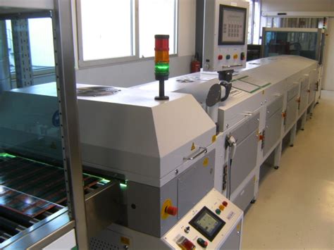
Soldermask Exposure Equipment and Process
Exposing LPI soldermask requires high intensity UV light. This is typically done using a soldermask exposure machine, which contains UV lamps (mercury vapor or LED) and a vacuum frame to hold the PCB and phototool in tight contact.
The key steps in the soldermask exposure process are:
-
Soldermask application – The liquid soldermask is applied to the PCB by curtain coating, screen printing, or spraying to the desired thickness (typically 0.5-1 mils). The board is then pre-baked to partially dry/set the soldermask.
-
Phototool placement – A phototool (photographic film or glass/quartz with a chrome pattern) is placed over the PCB, with the artwork aligned to the copper pattern. The phototool has clear areas where the soldermask needs to be removed (solder pads, SMT lands, tooling holes, etc.) and dark areas where the soldermask needs to remain.
-
Vacuum draw-down – The PCB and phototool are placed in the exposure unit’s vacuum frame, and a vacuum is pulled to ensure tight contact between the board and tool. This is critical to minimize undercutting and achieve fine resolution.
-
Exposure – The PCB is exposed to high intensity UV light for a certain duration (typically 30-60 seconds per side). The UV light crosslinks and hardens the soldermask polymer in the areas not masked by the phototool artwork.
-
Development – After exposure, the PCB is placed in a soldermask developer solution (typically 1-3% sodium or potassium carbonate). This dissolves away the unexposed soldermask, revealing the desired openings. The board is then rinsed and dried.
-
Final cure – To achieve full hardness and chemical resistance, the soldermask is given a final thermal cure, typically 60-90 minutes at 150°C.
The exposure energy (intensity x time) is one of the most critical parameters in this process. Too little exposure will result in soldermask that is underpolymerized and doesn’t develop out properly. Too much exposure can cause the fine lines and spaces in the artwork to fill in, leading to solder bridging. The optimal exposure energy depends on the soldermask material, thickness, and phototool artwork, but a typical starting point is around 200-400 mJ/cm2.

Optimizing and Troubleshooting Soldermask Exposure
Achieving consistent, high-quality soldermask requires careful control and optimization of the exposure parameters and conditions. Some key factors to consider include:
Exposure Energy
As mentioned, the exposure energy needs to be optimized for the specific soldermask material, thickness, and artwork. The soldermask supplier will typically provide a recommended exposure energy range, but it’s always best to run an exposure energy matrix to determine the optimal setting. This involves running a series of exposures at different energy levels and evaluating the resulting soldermask quality (resolution, adhesion, surface finish, etc.).
Artwork Quality
The phototool artwork needs to be of high quality to achieve the best soldermask printing. Some key artwork requirements include:
- Sufficient dark/clear contrast (typically > 3.0 OD)
- Sharp edges and corners (no blur or fuzziness)
- Correct polarity (clear pads for positive-acting soldermask)
- No scratches, pinholes, or other defects
- Dimensional accuracy and stability
Vacuum Contact
Intimate contact between the phototool and PCB surface is essential to minimize undercutting and achieve fine pitch resolution. The vacuum frame should be able to pull at least 25 in-Hg of vacuum, and the PCB and tool should be held flat and parallel. Any wrinkles, bubbles, or foreign matter can cause localized exposure issues.
Soldermask Thickness
The soldermask thickness needs to be well-controlled to achieve consistent exposure and development. If the soldermask is too thin, it may not provide adequate coverage and protection. If it’s too thick, it may not expose and develop properly, especially in fine pitch areas. The optimal thickness depends on the soldermask material and application requirements, but a typical range is 0.5-1 mils (12.5-25 μm).
Developer Concentration and Time
The soldermask developer solution needs to be at the correct concentration and temperature to effectively dissolve the unexposed polymer without attacking the exposed areas. The optimal concentration depends on the soldermask material, but a typical range is 1-3% sodium or potassium carbonate. The development time is usually 30-90 seconds, but this needs to be optimized based on the exposure energy and desired resolution.
Some common soldermask exposure defects and their causes include:
| Defect | Possible Causes |
|---|---|
| Incomplete development | Underexposure, weak developer, cold developer temp |
| Rough/blistered surface | Overexposure, contaminated developer, high humidity |
| Poor adhesion | Underexposure, contaminated copper surface, insufficient pre-bake |
| Solder bridging | Overexposure, artwork defects, insufficient vacuum |
| Inconsistent color | Uneven exposure or development, variable thickness |

Frequently Asked Questions (FAQ)
What is the difference between dry film and liquid photoimageable soldermask?
Dry film soldermask (DFSM) is a solid photopolymer film that is laminated to the PCB surface, while liquid photoimageable soldermask (LPISM) is a liquid that is applied by coating or spraying. LPISM is more common due to its better conformance and finer pitch resolution.
What is the best color for soldermask?
Green is the most common soldermask color, but other colors like blue, black, red, yellow, and white are also available. The choice of color is mostly cosmetic, but there can be some slight differences in opacity and thermal absorption.
Can soldermask be removed and reworked?
Yes, soldermask can be chemically stripped using strong alkaline solutions or abrasively removed by scrubbing or sandblasting. However, this is not recommended unless absolutely necessary, as it can damage the underlying circuitry. It’s better to prevent defects with proper process control.
How does soldermask affect the impedance of PCB traces?
Soldermask has a slight effect on the impedance of PCB traces, as it changes the dielectric constant of the surrounding medium. However, this effect is relatively minor (typically < 5% impedance change) and can be compensated for in the PCB design stage.
What is the shelf life of liquid photoimageable soldermask?
Most LPI soldermasks have a shelf life of 6-12 months when stored properly (cool, dark, dry environment). However, it’s best to use the soldermask as soon as possible for optimal performance and consistency. Expired soldermask can suffer from reduced photosensitivity, poor adhesion, and other issues.
In summary, proper exposure is crucial to achieving high-quality, reliable soldermask on PCBs. By understanding the key materials, equipment, and process parameters involved, and by carefully optimizing and controlling the exposure conditions, PCB manufacturers can produce boards with excellent soldermask definition, adhesion, and protection. While soldermask exposure can be challenging, getting it right pays off in the form of better-yielding, better-performing electronic products.


Leave a Reply