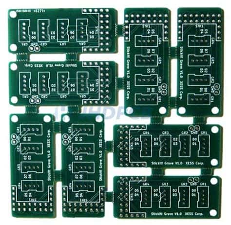
What is PCB Panelization?
PCB panelization is the process of grouping multiple printed circuit board designs onto a single panel for manufacturing. This technique is used to increase production efficiency and reduce manufacturing costs. By panelizing PCBs, manufacturers can produce a larger number of boards in a single run, minimizing the time and resources required for setup and handling.
Benefits of PCB Panelization
- Cost reduction
- Increased production efficiency
- Simplified handling and assembly
- Improved quality control
Challenges in Panelizing Round Shaped PCBs
Panelizing round shaped PCBs presents unique challenges compared to rectangular or square boards. Some of the difficulties include:
- Inefficient material utilization
- Increased complexity in panel design
- Difficulty in maintaining consistent spacing between boards
- Potential for damage during depanelization
Despite these challenges, it is still possible to effectively panelize round shaped PCBs with proper planning and execution.

Techniques for Panelizing Round Shaped PCBs
1. Tab Routing
Tab routing involves connecting the round PCBs to the panel using small tabs. These tabs are designed to be easily broken off after the manufacturing process is complete. When using tab routing, consider the following:
- Tab size and thickness
- Number and placement of tabs
- Material properties and breakaway strength
2. V-Scoring
V-scoring is a method of creating grooves or scores along the perimeter of the round PCBs. These grooves make it easier to separate the individual boards from the panel after manufacturing. When implementing V-scoring, keep in mind:
- Depth and angle of the V-score
- Material properties and thickness
- Potential for stress concentration and cracking
3. Perforated Routing
Perforated routing involves creating a series of small holes or perforations along the outline of the round PCBs. This technique allows for easy separation of the boards while maintaining the structural integrity of the panel during manufacturing. When using perforated routing, consider:
- Hole size, spacing, and pattern
- Material properties and thickness
- Balancing ease of separation with panel stability
4. Combination Techniques
In some cases, a combination of tab routing, V-scoring, and perforated routing may be used to optimize the panelization of round shaped PCBs. By leveraging the strengths of each technique, manufacturers can create panels that are efficient, stable, and easy to depanelize.

Design Considerations for Round Shaped PCB Panelization
When designing panels for round shaped PCBs, several factors must be taken into account to ensure optimal results:
- Material selection
- Choose materials with appropriate strength and breakaway properties
-
Consider the impact of material thickness on panelization techniques
-
Panel layout and spacing
- Optimize panel layout to maximize material utilization
-
Maintain consistent spacing between boards to ensure proper manufacturing
-
Tooling and depanelization
- Select appropriate tooling for the chosen panelization technique
-
Plan for efficient and safe depanelization methods
-
Design for manufacturing (DFM)
- Adhere to DFM guidelines to minimize potential issues during production
- Collaborate with manufacturers to ensure design compatibility with their processes

Best Practices for Round Shaped PCB Panelization
To achieve the best results when panelizing round shaped PCBs, consider the following best practices:
- Early collaboration with manufacturers
- Engage with manufacturers early in the design process
-
Discuss panelization options and constraints to optimize the design
-
Thorough testing and prototyping
- Conduct thorough testing of panelization techniques and designs
-
Create prototypes to validate the manufacturing process and identify potential issues
-
Continuous improvement and optimization
- Monitor the manufacturing process and gather feedback from stakeholders
- Continuously improve and optimize the panelization design based on data and insights
Common Pitfalls to Avoid in Round Shaped PCB Panelization
When panelizing round shaped PCBs, be aware of the following common pitfalls:
- Insufficient spacing between boards
- Inadequate spacing can lead to manufacturing defects and difficulty in depanelization
-
Ensure consistent and appropriate spacing based on the chosen panelization technique
-
Improper tab or perforation design
- Poorly designed tabs or perforations can result in damaged boards or difficulty in separation
-
Follow best practices and manufacturer guidelines when designing tabs and perforations
-
Neglecting material properties
- Failing to consider the properties of the PCB Material can lead to issues with panelization and depanelization
-
Select materials that are compatible with the chosen panelization technique and meet the required specifications
-
Lack of communication with manufacturers
- Poor communication with manufacturers can result in design incompatibilities and production delays
- Maintain open lines of communication and collaborate closely with manufacturers throughout the design and production process
Frequently Asked Questions (FAQ)
- What is the most suitable panelization technique for round shaped PCBs?
-
The most suitable panelization technique depends on factors such as the PCB design, material properties, and manufacturing requirements. Tab routing, V-scoring, and perforated routing are all viable options, and a combination of techniques may be used to achieve the best results.
-
How can I maximize material utilization when panelizing round shaped PCBs?
-
To maximize material utilization, optimize the panel layout by arranging the round PCBs in a tessellating pattern. This helps minimize the amount of wasted material between boards. Additionally, consider using smaller tabs or perforations to reduce the space required for separation.
-
What should I consider when selecting materials for round shaped PCB panelization?
-
When selecting materials, consider factors such as the strength, breakaway properties, and compatibility with the chosen panelization technique. The material thickness can also impact the effectiveness of tabs, V-scores, or perforations. Consult with manufacturers and material suppliers to select the most appropriate material for your specific application.
-
How can I ensure consistent spacing between round PCBs on a panel?
-
To ensure consistent spacing, use CAD tools to precisely layout the PCBs on the panel. Incorporate guidelines and measurements to maintain uniform gaps between boards. Additionally, communicate closely with manufacturers to ensure that the design is compatible with their processes and equipment.
-
What are the key steps to avoid damage during the depanelization of round shaped PCBs?
- To avoid damage during depanelization, follow these key steps:
- Choose an appropriate panelization technique that allows for easy and clean separation of the boards.
- Design tabs, V-scores, or perforations according to best practices and manufacturer guidelines to minimize stress concentration and cracking.
- Use specialized depanelization tools and equipment to ensure controlled and precise separation.
- Provide clear instructions and guidelines to the manufacturing team to ensure proper handling and depanelization procedures are followed.
By understanding the challenges, techniques, and best practices associated with panelizing round shaped PCBs, designers and manufacturers can work together to create efficient and cost-effective panels that meet the required specifications. Through early collaboration, thorough testing, and continuous improvement, the panelization process can be optimized to deliver high-quality round shaped PCBs consistently.
Conclusion
Panelizing round shaped PCBs presents unique challenges, but with the right techniques and best practices, it is possible to achieve efficient and cost-effective manufacturing. By selecting appropriate panelization methods, optimizing panel layouts, and collaborating closely with manufacturers, designers can overcome the difficulties associated with round PCB panelization.
As the demand for round shaped PCBs continues to grow in various industries, it is essential for designers and manufacturers to stay up-to-date with the latest panelization techniques and best practices. By embracing innovative solutions and continuously improving the panelization process, the electronics industry can meet the evolving needs of customers while maintaining high quality and cost-effectiveness.


Leave a Reply