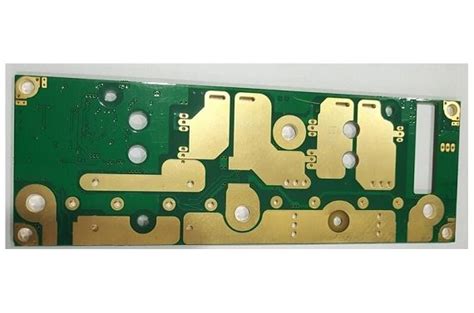
Understanding PCB Plating
Before delving into the cheapest plating material, let’s first understand what PCB plating is and why it is necessary. PCB plating involves depositing a thin layer of metal onto the copper traces and pads of the circuit board. This process serves several purposes:
- Protecting the copper from oxidation and corrosion
- Enhancing the solderability of the copper surfaces
- Improving the electrical conductivity of the connections
- Providing a durable and wear-resistant surface
PCB plating is typically done using electroplating or electroless plating techniques. Electroplating involves applying an electric current to deposit the metal ions onto the copper surfaces, while electroless plating relies on chemical reactions to achieve the same result.
Common PCB plating materials
There are several materials commonly used for PCB plating, each with its own characteristics and cost implications. Let’s take a look at some of the most popular options:
Gold Plating
Gold plating is known for its excellent corrosion resistance, high conductivity, and superior solderability. It is often used in high-reliability applications, such as aerospace, military, and medical devices. However, gold plating is also the most expensive option due to the high cost of the precious metal.
Silver Plating
Silver plating offers good conductivity and solderability at a lower cost compared to gold. It is sometimes used as an alternative to gold in less demanding applications. However, silver is prone to tarnishing and may require additional protection against oxidation.
Nickel Plating
Nickel plating is commonly used as an undercoat for other plating materials, such as gold or tin. It provides a barrier layer that prevents copper migration and improves the adhesion of the final plating layer. Nickel plating is relatively inexpensive compared to precious metals but lacks the same level of conductivity and corrosion resistance.
Tin Plating
Tin plating is one of the most widely used and cost-effective options for PCB plating. It offers good solderability, conductivity, and corrosion resistance at a fraction of the cost of gold or silver. Tin plating is often used in consumer electronics and other cost-sensitive applications.

The Cheapest Material for PCB Plating: Tin
Among the common PCB plating materials, tin stands out as the cheapest option. Tin plating provides several advantages that make it a popular choice for cost-conscious PCB manufacturers and designers.
Advantages of Tin Plating
-
Cost-effectiveness: Tin is significantly cheaper than precious metals like gold and silver, making it an attractive option for budget-constrained projects.
-
Good solderability: Tin-plated surfaces exhibit excellent solderability, allowing for reliable and strong solder joints.
-
Adequate conductivity: While not as conductive as gold or silver, tin still provides sufficient electrical conductivity for most PCB applications.
-
Corrosion resistance: Tin offers reasonable corrosion resistance, protecting the copper traces from oxidation and environmental factors.
-
Compatibility with lead-free soldering: Tin is compatible with lead-free soldering processes, which is important for compliance with environmental regulations.
Disadvantages of Tin Plating
Despite its cost advantages, tin plating does have some drawbacks that should be considered:
-
Whisker growth: Tin is prone to the formation of whiskers, which are thin, hair-like protrusions that can grow from the plated surface over time. Whiskers can cause short circuits and reliability issues if not properly controlled.
-
Lower durability: Compared to harder metals like nickel or gold, tin is relatively soft and may be more susceptible to wear and abrasion.
-
Limited high-frequency performance: Tin may not be the best choice for high-frequency applications due to its lower conductivity compared to gold or silver.

Tin Plating Techniques
Tin plating can be applied using different techniques, each with its own advantages and considerations. Let’s explore two common methods:
Hot Air Solder Leveling (HASL)
HASL is a popular tin plating technique that involves dipping the PCB into a molten solder bath and then using hot air to level the solder on the surface. The process results in a thin, uniform layer of tin-lead or lead-free solder on the copper pads and traces.
Advantages of HASL:
– Cost-effective and widely available
– Good solderability and wettability
– Suitable for most general-purpose PCB applications
Disadvantages of HASL:
– Limited flatness and coplanarity of the solder surface
– Potential for solder bridging or shorts
– Not suitable for fine-pitch components or high-density designs
Immersion Tin Plating
Immersion tin plating is a chemical process that deposits a thin layer of pure tin onto the copper surfaces without the use of electricity. The PCB is immersed in a tin solution, and the tin ions replace the copper ions on the surface through a displacement reaction.
Advantages of Immersion Tin:
– Produces a thin, uniform tin layer
– Suitable for fine-pitch components and high-density designs
– Excellent solderability and wettability
– Flat and coplanar surface finish
Disadvantages of Immersion Tin:
– Higher cost compared to HASL
– Limited shelf life due to the growth of tin oxide on the surface
– May require additional surface treatments for long-term storage

Cost Comparison of PCB Plating Materials
To provide a clearer picture of the cost differences between various PCB plating materials, let’s compare them in a table:
| Plating Material | Relative Cost | Typical Thickness |
|---|---|---|
| Gold | Very High | 0.05 – 0.2 μm |
| Silver | High | 0.2 – 0.5 μm |
| Nickel | Moderate | 1 – 5 μm |
| Tin (HASL) | Low | 1 – 25 μm |
| Tin (Immersion) | Low to Moderate | 0.5 – 1.5 μm |
As evident from the table, tin plating, both HASL and immersion tin, offers the lowest cost among the common PCB plating materials. The actual cost will depend on factors such as the PCB manufacturer, the specific plating process, and the volume of production.
Factors Affecting the Choice of PCB Plating Material
While cost is a significant consideration, there are other factors that influence the selection of the PCB plating material. These include:
-
Application requirements: The intended use of the PCB, such as high-reliability, high-frequency, or harsh environments, may dictate the choice of plating material.
-
Component compatibility: Some components, like fine-pitch or BGA packages, may require specific surface finishes for optimal solderability and reliability.
-
Manufacturing capabilities: The available plating processes and equipment at the PCB manufacturer may limit the choice of plating materials.
-
Environmental regulations: Compliance with lead-free and other environmental regulations may necessitate the use of certain plating materials.
-
Cost-performance trade-off: In some cases, a slightly more expensive plating material may be justified if it provides significant performance or reliability benefits.
Conclusion
In conclusion, tin plating emerges as the cheapest material for PCB plating, offering a cost-effective solution for many applications. Tin provides good solderability, adequate conductivity, and reasonable corrosion resistance at a lower cost compared to precious metals like gold and silver.
However, it is essential to consider the specific requirements of the PCB application and weigh the advantages and disadvantages of tin plating against other factors such as reliability, component compatibility, and manufacturing capabilities. In some cases, investing in a higher-cost plating material may be justified to ensure optimal performance and long-term reliability.
Ultimately, the choice of PCB plating material should be based on a careful evaluation of the project’s requirements, budget, and performance goals. Consultation with experienced PCB manufacturers and designers can help in making an informed decision that balances cost and performance considerations.
Frequently Asked Questions (FAQ)
-
Q: Is tin plating suitable for all PCB applications?
A: Tin plating is suitable for many general-purpose PCB applications, but it may not be the best choice for high-reliability, high-frequency, or harsh environment applications. It is essential to consider the specific requirements of the application when selecting the plating material. -
Q: What is the difference between HASL and immersion tin plating?
A: HASL (Hot Air Solder Leveling) involves dipping the PCB in a molten solder bath and using hot air to level the solder on the surface. Immersion tin plating is a chemical process that deposits a thin layer of pure tin onto the copper surfaces without the use of electricity. HASL is more cost-effective but may have limitations in terms of flatness and fine-pitch compatibility, while immersion tin provides a flatter surface finish but may be slightly more expensive. -
Q: Can tin plating be used for lead-free soldering?
A: Yes, tin plating is compatible with lead-free soldering processes. In fact, tin is a common component in lead-free solder alloys, such as SAC (tin-silver-copper) alloys. -
Q: What is the typical thickness of tin plating on PCBs?
A: The thickness of tin plating depends on the specific plating technique used. HASL typically results in a thickness of 1-25 μm, while immersion tin plating produces a thinner layer of 0.5-1.5 μm. -
Q: How does tin plating compare to other materials in terms of shelf life?
A: Tin-plated surfaces have a limited shelf life compared to other materials like gold or nickel. Over time, tin can develop an oxide layer that affects its solderability. Proper storage conditions and additional surface treatments can help extend the shelf life of tin-plated PCBs.


Leave a Reply