Introduction to Layout and Schematic Design
When it comes to electronic circuit design, the schematic and layout are two essential components that work hand in hand. The schematic represents the logical connections between components in a circuit, while the layout is the physical representation of how those components will be arranged on a printed circuit board (PCB). In this article, we will delve into the process of creating a layout from a schematic, exploring the best practices, tools, and techniques to ensure a successful PCB design.
Understanding the Schematic
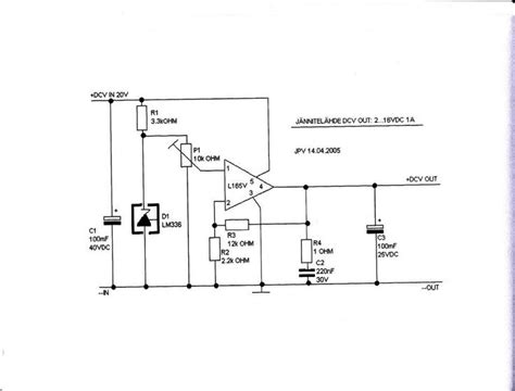
A schematic is a graphical representation of an electronic circuit, showcasing the interconnections between various components such as resistors, capacitors, integrated circuits (ICs), and more. It serves as a blueprint for the circuit, allowing designers to visualize the logical flow of signals and power. Schematics use standardized symbols to represent each component, making it easy for engineers to interpret the circuit’s functionality.
The Importance of a Well-Designed Layout
While the schematic captures the logical aspects of a circuit, the layout is responsible for translating that logic into a physical form that can be manufactured as a PCB. A well-designed layout is crucial for several reasons:
-
Signal Integrity: The layout determines how signals propagate through the circuit. Proper routing and component placement help minimize signal integrity issues such as crosstalk, reflections, and electromagnetic interference (EMI).
-
Power Distribution: The layout plays a vital role in ensuring proper power distribution throughout the circuit. Adequate copper pour and proper placement of power and ground planes help maintain stable voltage levels and minimize voltage drops.
-
Manufacturability: A layout designed with manufacturability in mind reduces the chances of fabrication issues and improves yield. This includes considerations such as component spacing, trace widths, and clearances.
-
Thermal Management: The layout influences how heat is dissipated from components. Proper thermal management helps prevent overheating and ensures the long-term reliability of the circuit.
Step-by-Step Guide to Creating a Layout from a Schematic
Now that we understand the importance of a well-designed layout, let’s walk through the steps involved in creating a layout from a schematic.
Step 1: Schematic Review and Verification
Before starting the layout process, it’s crucial to thoroughly review and verify the schematic. This step involves:
-
Checking for completeness: Ensure that all necessary components and connections are present in the schematic.
-
Verifying component values: Double-check the values of components such as resistors, capacitors, and inductors to ensure they match the design requirements.
-
Confirming pin assignments: Verify that the pin assignments of ICs and other components are correct and match the datasheet specifications.
-
Identifying critical signals: Make note of critical signals such as clocks, high-speed interfaces, and sensitive analog signals that may require special attention during layout.
Step 2: Component Placement
Once the schematic is verified, the next step is to place the components on the layout. Component placement is a critical aspect of layout design, as it directly impacts signal integrity, power distribution, and thermal management. Here are some guidelines to follow:
-
Group related components: Place components that are functionally related or have high interconnectivity close together to minimize trace lengths and improve signal integrity.
-
Consider signal flow: Arrange components in a logical sequence that follows the signal flow from input to output. This helps minimize crossing traces and reduces the chances of signal interference.
-
Separate analog and digital sections: If the circuit has both analog and digital sections, it’s important to separate them to minimize noise coupling. Use ground planes or guard rings to provide isolation between the two domains.
-
Optimize for thermal management: Place components that generate significant heat, such as power regulators or high-power ICs, in areas with good thermal dissipation. Consider using thermal vias or heatsinks if necessary.
-
Accommodate mechanical constraints: Take into account any mechanical constraints such as connector locations, mounting holes, or enclosure dimensions when placing components.
Step 3: Routing the Traces
After component placement, the next step is to route the traces that connect the components together. Routing is the process of creating the copper paths on the PCB that carry signals and power between components. Here are some best practices for routing:
-
Use appropriate trace widths: Select trace widths based on the current carrying requirements and the desired impedance of the signals. Wider traces have lower resistance and can carry more current, while narrower traces are suitable for high-speed signals.
-
Minimize trace lengths: Keep traces as short as possible to reduce signal delays, minimize parasitic effects, and improve signal integrity. Avoid unnecessary meandering or long routes.
-
Avoid sharp angles: Use 45-degree angles or curved traces instead of 90-degree angles to minimize signal reflections and improve manufacturability.
-
Maintain proper clearances: Ensure that traces maintain the minimum required clearance from other traces, components, and the board edge to avoid short circuits and manufacturing issues.
-
Consider differential pairs: When routing high-speed differential signals, such as USB or Ethernet, ensure that the traces are routed as a closely coupled pair with matched lengths to maintain signal integrity.
-
Utilize ground planes: Use ground planes to provide a low-impedance return path for signals and to minimize EMI. Ensure that the ground plane is properly connected to the components and has adequate vias for stitching.
Step 4: Power Distribution
Proper power distribution is essential for the stable operation of the circuit. Here are some considerations for power distribution in the layout:
-
Use appropriate copper pour: Provide adequate copper pour for power and ground planes to ensure low-impedance power distribution. The thickness of the copper pour depends on the current requirements of the circuit.
-
Decouple power supplies: Place decoupling capacitors close to the power pins of ICs to minimize power supply noise and provide a stable voltage reference.
-
Use power and ground planes: Dedicate separate layers for power and ground planes to minimize impedance and provide a low-inductance path for current flow.
-
Consider voltage drops: Ensure that the voltage drop across the power traces is within acceptable limits. Use wider traces or multiple vias for high-current paths to minimize voltage drops.
Step 5: Design Rule Check (DRC) and Final Review
Before sending the layout for fabrication, it’s essential to perform a thorough design rule check (DRC) and final review. The DRC verifies that the layout adheres to the manufacturing constraints and design rules specified by the PCB fabricator. It checks for issues such as minimum trace widths, clearances, and hole sizes.
After passing the DRC, conduct a final visual inspection of the layout. Look for any obvious errors, such as missing connections or incorrect Component orientations. It’s also a good practice to have a colleague or peer review the layout to catch any potential issues.

Tools for Layout Design
There are various software tools available for creating layouts from schematics. Some popular options include:
-
Altium Designer: A comprehensive PCB design software that offers schematic capture, layout design, and 3D visualization capabilities.
-
KiCad: An open-source PCB design suite that provides schematic capture, layout design, and simulation features.
-
EAGLE: A widely used PCB design software that offers schematic capture, layout design, and an extensive component library.
-
OrCAD: A powerful PCB design solution that includes schematic capture, layout design, and simulation tools.
These tools provide a range of features and capabilities to streamline the layout design process, such as auto-routing, design rule checking, and 3D visualization.

Best Practices for Layout Design
To ensure a successful layout design, consider the following best practices:
-
Start with a good schematic: A well-designed schematic is the foundation for a good layout. Ensure that the schematic is complete, accurate, and properly organized.
-
Plan your stackup: Determine the number of layers and the layer stackup early in the design process. This helps in properly assigning components and routing traces.
-
Use a consistent grid: Establish a consistent grid for component placement and trace routing. This helps maintain a neat and organized layout and improves manufacturability.
-
Keep it simple: Avoid unnecessary complexity in the layout. Keep the design as simple and straightforward as possible to minimize the chances of errors and improve reliability.
-
Document your design: Maintain proper documentation of your layout, including layer assignments, component placement rationale, and any special considerations. This helps in future revisions and troubleshooting.

Frequently Asked Questions (FAQ)
- What is the difference between a schematic and a layout?
-
A schematic represents the logical connections between components in a circuit, while a layout is the physical representation of how those components are arranged on a PCB.
-
Why is component placement important in layout design?
-
Component placement directly impacts signal integrity, power distribution, and thermal management. Proper placement helps minimize signal interference, ensures stable power delivery, and prevents overheating.
-
What are the benefits of using ground planes in a layout?
-
Ground planes provide a low-impedance return path for signals, minimize EMI, and help maintain signal integrity. They also improve power distribution and provide shielding between different sections of the circuit.
-
How can I ensure manufacturability in my layout design?
-
To ensure manufacturability, consider factors such as component spacing, trace widths, clearances, and hole sizes. Adhere to the design rules specified by the PCB fabricator and perform a thorough design rule check (DRC) before sending the layout for fabrication.
-
What should I do if I encounter signal integrity issues in my layout?
- If you encounter signal integrity issues, review your component placement and trace routing. Ensure that critical signals are properly routed, maintain appropriate trace widths and spacing, and use techniques such as ground planes and shielding to minimize interference. Perform signal integrity simulations to identify and address any potential issues.
Conclusion
Creating a layout from a schematic is a critical step in the PCB design process. By following best practices and utilizing the right tools, you can transform your schematic into a well-designed layout that ensures signal integrity, power distribution, and manufacturability. Remember to start with a good schematic, plan your stackup, use a consistent grid, keep it simple, and document your design. By paying attention to the details and adhering to industry standards, you can create layouts that are reliable, efficient, and ready for fabrication.


Leave a Reply