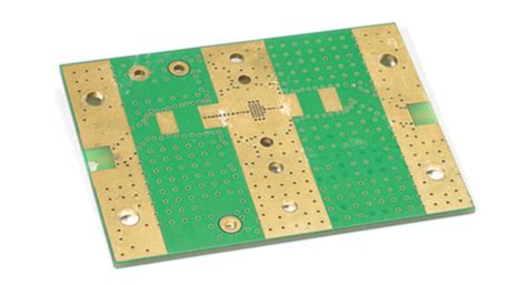
Key features found on the PCB Bottom
Solderpads
Solderpads, also known as footprints or land patterns, are exposed metal areas on the bottom of the PCB where components leads are soldered. The size, shape and spacing of the pads match the component package so it can be properly soldered in place. Some common types of solderpads on PCB bottoms include:
| Pad Type | Description |
|---|---|
| SMD | Surface mount pads for SMD components |
| Thru-hole | Pads with holes for through-hole component leads |
| BGA | Grid of small round pads for ball grid array packages |
| Connector | Larger pads for connector pins |
Having the appropriate solderpads is essential for reliable solder joints. The pads must be the correct size – not too small which could result in insufficient solder, or too large causing solder bridges. Pad shape and spacing is also important to match the component and allow room for soldering.
Solder mask
The solder mask is a thin protective layer that covers the bottom of the PCB except for the exposed solderpads and other areas that require soldering. It is typically green in color but can also be red, blue, black, white or yellow. The main purposes of solder mask on the PCB bottom are:
- Prevents solder bridges by restricting solder to just the pads
- Protects the copper traces from oxidation and corrosion
- Provides electrical insulation between adjacent traces
- Improves PCB aesthetics and readability of silkscreen text
Solder mask is applied to the PCB bottom using photolithography and then cured. Everywhere the mask is removed exposes the underlying bare copper, forming the solderpads. A high quality and properly patterned solder mask is important for good solderability and reliability of the bottom side.
Copper traces
Copper traces are the thin lines of copper that form the electrical connections between components on different layers of the PCB. On the bottom side, traces connect the solderpads to vias which link to traces on other layers to complete circuits.
The traces on PCB bottoms must be carefully designed and fabricated to ensure:
- Correct trace widths for current carrying capacity
- Proper spacing between traces to avoid unintended shorts
- Good solderability at the trace to pad transitions
- Minimal inductance and impedance for high speed signals
- Efficient routing to minimize trace lengths and use available space
For complex, high-density PCB designs, the traces on the bottom side are often narrow (3-4 mils) and closely spaced. This requires precision manufacturing processes to avoid defects like open or shorted traces. The bottom side traces play a critical role in PCB performance and reliability.
Vias
Vias are small holes drilled through the PCB to connect traces on different layers. They are essential for routing circuits in multi-layer PCB designs. On the bottom side, vias appear as round pads similar to thru-hole pads but smaller. The most common types of vias seen on PCB bottoms are:
- Thru vias that go through all layers
- Blind vias that connect the bottom to one or more inner layers
- Buried vias that connect inner layers without being visible on top or bottom
Micro vias are increasingly used on high density PCBs. These are very small vias, typically laser drilled, that can connect to finer pitch pads and traces. Via-in-pad is another technique where the via is placed in the SMD pad to save space.
Having properly fabricated and cleaned vias is important for making good connections between layers. Improperly drilled or plugged vias can cause open circuits. Vias also impact signal integrity and must be carefully designed in high speed layouts.
Silkscreen
The silkscreen is the text and graphics printed on the solder mask of the PCB bottom. It is typically white but can be other colors. The main purpose is to label components, connectors, test points, and other features for easier assembly and servicing.
Common information found in the bottom side silkscreen includes:
- Reference designators for each component
- Polarity marks for diodes, electrolytic caps, ICs
- Pin 1 indication for IC packages
- Connector pinouts and key orientation
- Company name, logo, part number, version
- Manufacturing marks like UL, RoHS, date code
- Test points, LEDs, buttons, switches, etc.
Having clear, readable and properly positioned silkscreen is important for manual PCB Assembly and visual inspection. The silkscreen must not overlap pads which could affect soldering. Locating silkscreen away from large components also improves legibility.
Test points
Test points are dedicated pads or vias on the PCB used for testing and debugging the assembled board. They allow probing of key signals or voltage rails without having to touch component pins. On the bottom side, test points are often located near the edge of the board for easy access.
Types of bottom side test points include:
- Probeable vias connected to inner layer signals
- SMD pads for test clips or pogo pins
- Plated through-holes for post assembly soldering of wires
Designing in test points on the PCB bottom can greatly improve testability. They are used in flying probe and bed of nails testing to verify solder joints and basic functionality. Having accessible test points also speeds up debugging and failure analysis. The size, location and spacing of test points must be carefully planned.
PCB bottom assembly process
The PCB bottom is the main side for surface mount assembly since most SMD packages are mounted there. A typical process for bottom side PCB assembly is:
- Apply solder paste to the pads via stencil printing
- Automated pick and place of SMD components
- Solder reflow in conveyor oven to melt paste and form joints
- Inspection of solder joints and components (AOI, X-ray)
- Manual soldering of any thru-hole parts inserted from bottom
- Test and debug using bottom side test points
Wave soldering or selective soldering may also be used after reflow if there are many through-hole parts on the bottom side.
Proper design and fabrication of the PCB bottom is critical for a smooth assembly process. Issues like solder mask misalignment, insufficient or excessive solder, poor hole plating, etc. will cause defects and re-work.

Inspection and testing of PCB bottom
Inspecting and testing the assembled PCB bottom is important for identifying any manufacturing defects or assembly issues. Common techniques used include:
- Manual visual inspection with microscope to check solder joints, component placement
- Automated optical inspection (AOI) to detect missing parts, wrong values, poor soldering
- X-ray inspection to see solder joints under BGA and QFN packages
- Flying probe test to verify continuity and basic functionality
- In-circuit test (ICT) with bed of nails fixture to do detailed analog testing
- Functional test to validate operation and performance
Designing the PCB bottom with testing in mind, such as having sufficient test points and probe access, can greatly facilitate inspection and debug. Catching any issues at this stage prevents defective boards from progressing to later stages where re-work is more difficult and costly.

Thermal considerations for PCB bottom
For PCBs with high power components, thermal management is an important consideration for the bottom side design. The large copper planes and traces needed to dissipate heat are typically placed on the bottom layer.
Techniques used for bottom side thermal management include:
- Maximizing the copper area of the power and ground planes
- Using wide and thick traces to connect to power hungry components
- Providing thermal relief pads and vias to help conduct heat to inner layers
- Locating hot components near board edges or away from thermally sensitive parts
- Specifying a thicker base copper layer (2-3 oz) for the PCB bottom
In some cases, additional heat sinking may be required, such as attaching metal backed PCBs to a chassis or using bottom mounted heatsinks and thermal pads. Thermal simulations and measurements can help validate the effectiveness of the thermal design.

Common PCB bottom issues and defects
Some common manufacturing issues and assembly defects that can occur on the PCB bottom include:
- Soldermask misregistration exposing traces or covering pads
- Insufficient or excessive solder paste printing
- Solder bridging or tombstoning of small SMD parts
- Poor hole plating leading to open vias or unreliable barrels
- Damaged or lifted pads from rough handling or rework
- Solder balls or splatter causing shorts
- Component misalignment or billboarding of large ICs
Many of these issues arise from problems with the bare board fabrication, such as incorrect etching or drilling, or poor solder mask application. Improper solder paste and component placement can also lead to defects during assembly.
Careful inspection of the PCB bottom at incoming and post-assembly can help identify these issues early. Addressing any problems with the bare board supplier or assembly process can improve quality and yield.
Advanced PCB bottom technologies
Some of the latest technologies and techniques being used for PCB bottom design include:
- High Density Interconnect (HDI) with micro vias and fine pitch traces
- Embedded components and printed electronics to reduce size and layer count
- Flex and rigid-flex circuits that can bend or fold for tight packaging
- Metal core or ceramic substrates for better thermal management
- Advanced surface finishes like immersion silver or gold for improved solderability
Many of these require specialized materials, processes and design rules beyond standard FR-4 PCBs. They offer advantages in terms of size, weight, performance and reliability but also come with added complexity and cost. Designers must carefully weigh the benefits and drawbacks when considering these advanced technologies for PCB bottoms.
FAQ
What is the difference between the top and bottom side of a PCB?
The top side, also known as the component side, is where most of the components are mounted and labeled. The bottom side has the solderpads, traces and other features needed to attach and connect the components. SMD parts are typically mounted on the bottom while through-hole parts are inserted from the top and soldered on the bottom.
Why is the solder mask on PCBs usually green?
Green is the most common color for solder mask as it provides good contrast for the white silkscreen, is easy to inspect, and is widely available and low cost. However, other colors like blue, red, black or yellow are sometimes used for aesthetic or functional reasons. The exact shade of green can also vary between manufacturers.
What is the minimum trace width and spacing on a PCB bottom?
The minimum trace width and spacing depends on the PCB fabricator and the capabilities of their process. For standard low-cost PCBs, 5-6 mil traces and spacing is common. For high-density designs, 3-4 mil traces and spacing are possible but require more advanced fabrication and higher costs. The trace width also depends on the required current carrying capacity.
How are vias fabricated on the PCB bottom?
Vias are mechanically drilled or laser drilled through the PCB substrate. The hole walls are then plated with copper to form a conductive barrel connecting the top and bottom layers. For multi-layer boards, additional copper plating is used to connect the inner layers. The via pads are exposed on the bottom solder mask to allow soldering.
What are some best practices for PCB bottom layout?
Some key guidelines for PCB bottom layout include:
- Providing adequate size and spacing for solderpads based on component package
- Ensuring solder mask registration to avoid exposed traces or covered pads
- Minimizing trace lengths and using sufficient width for current and impedance
- Providing thermal relief pads and vias for heat dissipation
- Placing test points and fiducials to facilitate inspection and testing
- Optimizing placement of SMD components for ease of assembly
- Following manufacturer’s design rules and guidelines for fabrication and assembly
By carefully designing the PCB bottom and working closely with the fabricator and assembler, many potential issues can be avoided and a high quality, reliable product can be achieved.
Conclusion
The bottom side of a PCB is a critical aspect of the design that requires careful attention to layout, manufacturing and assembly. It contains the key features like solderpads, traces and vias that connect and mount the components. Understanding the capabilities and limitations of PCB bottom fabrication and assembly processes is essential for designing a board that is high yield, reliable and testable.
As PCB technology continues to evolve, new techniques and materials are enabling more advanced bottom side designs with finer pitches, higher densities and better thermal performance. However, these require specialized knowledge and close collaboration between the designer, manufacturer and assembler.
By following best practices and leveraging the latest technologies, PCB designers can create bottom side layouts that meet the ever increasing demands of today’s electronic products. A well-designed and manufactured PCB bottom is essential for a successful product that functions and performs as intended.


Leave a Reply