Introduction to Inner PCB Layers
Printed Circuit Boards (PCBs) are essential components in modern electronic devices, providing a platform for interconnecting various electronic components. While the Outer Layers of a PCB are visible and often feature components and connectors, the inner layers play a crucial role in the overall functionality and performance of the board. In this article, we will delve into the world of inner PCB layers, exploring their purpose, composition, and the various types of inner layers used in PCB design.
What are Inner PCB Layers?
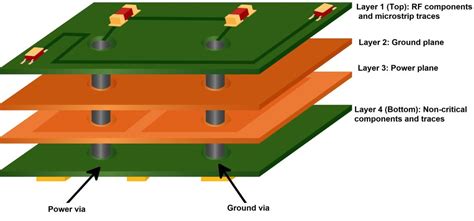
Inner PCB layers, also known as internal layers or buried layers, are the conductive layers sandwiched between the top and bottom layers of a multi-layer PCB. These layers are not visible from the outside and are embedded within the insulating substrate material, typically FR-4. The primary purpose of inner layers is to provide additional routing paths for electrical signals, power, and ground planes, allowing for more complex and compact PCB designs.
The Role of Inner Layers in PCB Design
Inner layers serve several essential functions in PCB design:
-
Signal Routing: Inner layers provide additional space for routing electrical signals between components on the PCB. By utilizing inner layers, designers can create more efficient and shorter signal paths, reducing the overall size of the PCB and improving signal integrity.
-
Power and Ground Distribution: Inner layers are often used as power and ground planes, providing a low-impedance path for distributing power and ground to various components on the board. These planes help to minimize voltage drops, reduce electromagnetic interference (EMI), and improve the overall power distribution network.
-
Shielding and Noise Reduction: Inner layers can be strategically placed to act as shielding layers, reducing the impact of electromagnetic interference (EMI) and crosstalk between adjacent signal layers. By separating sensitive signal layers with ground or power planes, designers can minimize noise and improve signal quality.
-
Increased Design Flexibility: The use of inner layers allows for more complex and compact PCB designs. With additional routing space and the ability to create blind and buried vias, designers can accommodate a higher component density and more intricate interconnections.
Types of Inner PCB Layers
Inner PCB layers can be classified into several categories based on their purpose and composition:
Signal Layers
Signal layers are used for routing electrical signals between components on the PCB. These layers typically consist of thin copper traces that carry signals from one point to another. The width and spacing of these traces are determined by factors such as the signal frequency, current requirements, and the desired characteristic impedance.
Power and Ground Planes
Power and ground planes are inner layers dedicated to distributing power and ground to the components on the PCB. These planes are typically solid copper layers that cover a significant portion of the board area. The power plane provides a low-impedance path for the supply voltage, while the ground plane serves as a reference for all signals and helps to minimize ground loops and noise.
Split Planes
Split planes are a variation of power and ground planes where the plane is divided into multiple sections, each serving a specific purpose. For example, a split power plane may have separate sections for different voltage levels, such as 3.3V and 5V. Split planes can help to isolate different power domains, reduce noise, and improve power integrity.
Shielding Layers
Shielding layers are inner layers that are strategically placed to reduce electromagnetic interference (EMI) and crosstalk between adjacent signal layers. These layers are typically solid copper planes that are connected to ground, creating a barrier that attenuates electromagnetic fields. Shielding layers are often used in high-speed digital designs or in applications where EMI is a concern.

Manufacturing Process of Inner PCB Layers
The manufacturing process of inner PCB layers involves several steps:
-
Layer Stack-up Design: The first step is to design the layer stack-up, which defines the number, type, and order of the inner layers. The stack-up design takes into account factors such as the required number of signal layers, power and ground distribution, and the desired thickness of the PCB.
-
Inner Layer Patterning: Once the stack-up is defined, the inner layers are patterned using a photolithography process. The copper-clad laminate is coated with a photoresist material, and the desired pattern is transferred onto the photoresist using a photomask and exposure to UV light. The unexposed photoresist is then removed, leaving the desired copper pattern on the inner layer.
-
Lamination: After the inner layers are patterned, they are stacked and aligned according to the layer stack-up design. The stack is then laminated under high pressure and temperature, bonding the layers together with the insulating substrate material, typically FR-4.
-
Drilling and Plating: Once the layers are laminated, holes are drilled through the PCB to create vias that connect the inner layers to the outer layers and to each other. The holes are then plated with copper to establish electrical connections between the layers.
-
Outer Layer Processing: Finally, the outer layers of the PCB are processed, which involves patterning, etching, and applying the solder mask and silkscreen.

Design Considerations for Inner PCB Layers
When designing inner PCB layers, several factors must be considered to ensure optimal performance and manufacturability:
Signal Integrity
Signal integrity is a critical consideration when designing inner layers. Factors such as trace width, spacing, and impedance control must be carefully chosen to minimize signal reflections, crosstalk, and other signal integrity issues. High-speed designs may require the use of controlled impedance traces and specific dielectric materials to maintain signal quality.
Power Integrity
Power integrity is another important aspect of inner layer design. The power and ground planes must be adequately sized and placed to minimize voltage drops and ensure a stable power supply to all components on the board. Proper decoupling and bypass capacitor placement are also essential for maintaining power integrity.
Thermal Management
Inner layers can also impact the thermal performance of the PCB. The placement of power and ground planes, as well as the overall layer stack-up, can affect the heat dissipation capabilities of the board. Thermal vias and other thermal management techniques may be necessary to ensure proper heat dissipation and prevent overheating of components.
Manufacturing Constraints
The design of inner layers must also consider manufacturing constraints, such as minimum trace width and spacing, hole sizes, and layer-to-layer registration tolerances. Designers must work closely with the PCB manufacturer to ensure that the design is compatible with their manufacturing capabilities and to minimize the risk of manufacturing defects.

Frequently Asked Questions (FAQ)
-
What is the purpose of inner layers in a PCB?
Inner layers in a PCB provide additional routing space for electrical signals, power, and ground distribution. They allow for more complex and compact PCB designs and can also be used for shielding and noise reduction. -
How many inner layers can a PCB have?
The number of inner layers in a PCB can vary depending on the complexity of the design and the manufacturing capabilities. PCBs can have anywhere from 2 to over 50 layers, with 4, 6, 8, and 10-layer boards being common configurations. -
What materials are used for inner PCB layers?
Inner PCB layers are typically made of copper-clad laminates, with the most common base material being FR-4. Other materials, such as high-frequency laminates or metal-core substrates, may be used for specific applications or to enhance thermal performance. -
How are inner layers connected to the outer layers of a PCB?
Inner layers are connected to the outer layers and to each other through vias. Vias are holes drilled through the PCB that are plated with copper to establish electrical connections between the layers. There are various types of vias, such as through-hole, blind, and buried vias, each serving different purposes in the PCB design. -
What are the challenges in designing inner PCB layers?
Designing inner PCB layers presents several challenges, including maintaining signal integrity, ensuring proper power distribution, and managing thermal performance. Designers must also consider manufacturing constraints and work closely with the PCB manufacturer to ensure the design is compatible with their capabilities and can be reliably produced.
Conclusion
Inner PCB layers are a critical component in modern PCB design, providing additional routing space, power and ground distribution, and shielding capabilities. Understanding the types of inner layers, their manufacturing process, and the design considerations involved is essential for creating high-performance and reliable PCBs.
As electronic devices continue to become more complex and compact, the role of inner PCB layers will only become more significant. By leveraging the benefits of inner layers and following best design practices, PCB designers can create more advanced and efficient electronic systems that meet the ever-increasing demands of the industry.
| Layer Type | Purpose | Composition |
|---|---|---|
| Signal Layers | Routing electrical signals between components | Thin copper traces |
| Power and Ground Planes | Distributing power and ground to components | Solid copper layers covering a significant portion of the board area |
| Split Planes | Isolating different power domains and reducing noise | Divided into multiple sections, each serving a specific purpose |
| Shielding Layers | Reducing electromagnetic interference (EMI) and crosstalk | Solid copper planes connected to ground |
In summary, inner PCB layers are a vital aspect of modern PCB design, offering numerous benefits and enabling the creation of more advanced and compact electronic devices. By understanding the types, manufacturing process, and design considerations of inner layers, PCB designers can create high-performance and reliable PCBs that meet the demands of today’s electronics industry.


Leave a Reply