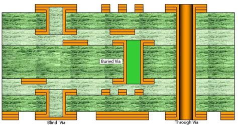
What are Blind Vias?
Blind vias are a type of interconnection used in multi-layer PCBs, where the via starts on an outer layer and terminates on an inner layer, without going through the entire board. Unlike through-hole vias, which are visible on both sides of the PCB, blind vias are only visible on one side of the board.
Types of Blind Vias
There are two main types of blind vias:
- Single-sided blind vias: These vias start from one outer layer and terminate on an inner layer.
- Double-sided blind vias: These vias start from both Outer Layers and terminate on inner layers, without connecting the outer layers to each other.
Advantages of Using Blind Vias
Blind vias offer several advantages in PCB Design, making them an essential tool for high-density layouts:
1. Space Savings
One of the primary benefits of using blind vias is the space savings they offer. By eliminating the need for through-hole vias, blind vias allow for a more compact PCB layout, enabling designers to place components closer together and reduce the overall board size.
2. Improved Signal Integrity
Blind vias can help improve signal integrity by reducing the via stub effect. Via stubs are the unused portions of a through-hole via that can cause signal reflections and degrade high-speed signal performance. By terminating on an inner layer, blind vias minimize the via stub length, resulting in cleaner signals and better overall performance.
3. Increased Routing Flexibility
With blind vias, PCB designers have more flexibility in routing traces on inner layers. This is particularly useful in high-density designs where space is limited, as it allows for more efficient use of board real estate and reduces the need for complex routing strategies.
4. Enhanced Thermal Management
Blind vias can also contribute to better thermal management in PCBs. By strategically placing blind vias near heat-generating components, designers can create Thermal Vias that help dissipate heat more effectively, preventing components from overheating and improving overall reliability.

Manufacturing Process for Blind Vias
The manufacturing process for blind vias is more complex than that of through-hole vias, requiring specialized equipment and techniques. The two main methods for creating blind vias are:
1. Controlled Depth Drilling
Controlled depth drilling involves using a precise drilling machine to create holes that stop at a specific depth within the PCB stack-up. This process requires careful control of drilling parameters, such as drill bit size, speed, and depth, to ensure accurate and consistent results.
2. Sequential Lamination
Sequential lamination is a process where the PCB is built up in stages, with each layer being laminated and drilled separately before being combined into the final stack-up. This allows for the creation of blind vias by drilling and plating the vias on individual layers before laminating them together.

Designing with Blind Vias
When incorporating blind vias into a PCB design, there are several factors to consider:
1. Stack-up Planning
Careful planning of the PCB stack-up is crucial when using blind vias. Designers must determine the optimal layer arrangement and thickness to accommodate blind vias while ensuring proper signal integrity and manufacturability.
2. Via Sizing and Placement
Blind vias should be sized appropriately based on the current carrying requirements and the capabilities of the manufacturing process. Designers should also consider the placement of blind vias to minimize signal reflections and ensure proper connectivity between layers.
3. Design Rule Checking (DRC)
Designers must ensure that their blind via designs comply with the manufacturing capabilities and design rules provided by the PCB fabricator. This involves running DRC checks to verify that via sizes, spacing, and layer assignments meet the specified requirements.

Buried Vias: Taking it a Step Further
While blind vias offer significant advantages in high-density PCB design, buried vias take the concept even further. Buried vias are similar to blind vias but are located entirely within the inner layers of the PCB, without connecting to either outer layer.
Advantages of Buried Vias
Buried vias offer several advantages over blind vias:
- Further space savings: By eliminating the need for any connection to the outer layers, buried vias allow for an even more compact PCB layout.
- Improved signal integrity: Buried vias have minimal impact on signal integrity, as they are isolated from the outer layers and have no exposed via stubs.
- Enhanced security: Since buried vias are not visible from the outer layers, they can provide an added layer of security for sensitive connections or intellectual property.
Manufacturing Challenges
However, the manufacturing process for buried vias is even more complex than that of blind vias. Creating buried vias requires a combination of controlled depth drilling and sequential lamination, with each layer being processed separately before being laminated together. This complexity increases the cost and lead time for PCBs with buried vias.
FAQ
Q: What is the difference between blind vias and buried vias?
A: Blind vias start from an outer layer and terminate on an inner layer, while buried vias are located entirely within the inner layers of the PCB, without connecting to either outer layer.
Q: Can blind vias improve signal integrity?
A: Yes, blind vias can help improve signal integrity by reducing the via stub effect, which minimizes signal reflections and enhances high-speed signal performance.
Q: Are blind vias more expensive than through-hole vias?
A: Yes, the manufacturing process for blind vias is more complex and requires specialized equipment, resulting in higher costs compared to through-hole vias.
Q: How do blind vias help with thermal management in PCBs?
A: By strategically placing blind vias near heat-generating components, designers can create thermal vias that help dissipate heat more effectively, improving overall thermal management and reliability.
Q: What factors should be considered when designing with blind vias?
A: When designing with blind vias, factors to consider include stack-up planning, via sizing and placement, and ensuring compliance with manufacturing capabilities and design rules through DRC checks.
Conclusion
Blind and buried vias are essential elements of high-density PCB design, offering numerous advantages over traditional through-hole vias. By enabling more compact layouts, improving signal integrity, and enhancing thermal management, these advanced via types allow designers to push the boundaries of PCB complexity and functionality.
However, the manufacturing processes for blind and buried vias are more complex and costly compared to through-hole vias, requiring specialized equipment and techniques. As such, designers must carefully weigh the benefits and costs when deciding whether to incorporate these via types into their PCB designs.
As electronic devices continue to shrink in size and increase in complexity, the use of blind and buried vias will likely become even more prevalent in the future. By understanding the advantages, challenges, and design considerations associated with these via types, PCB designers can create more efficient, reliable, and high-performance electronic products.
| Via Type | Description | Advantages | Manufacturing Complexity |
|---|---|---|---|
| Through-hole Via | Connects all layers, visible on both sides | Simple, low cost | Low |
| Blind Via | Connects outer layer to inner layer, visible on one side | Space savings, improved signal integrity, thermal management | Medium |
| Buried Via | Connects inner layers only, not visible on outer layers | Further space savings, enhanced signal integrity and security | High |


Leave a Reply