Introduction to PCB Identification
Printed Circuit Boards (PCBs) are the backbone of modern electronics. They provide a platform for electrical components to be connected and interact with each other. PCBs come in various shapes, sizes, and complexities, depending on their intended application. Proper identification of PCBs is crucial for manufacturers, engineers, and technicians to ensure compatibility, functionality, and maintainability. In this article, we will explore the various methods and characteristics used to identify PCBs.
PCB Identification Methods
There are several methods used to identify PCBs, each with its own advantages and limitations. The most common methods include:
1. Visual Inspection
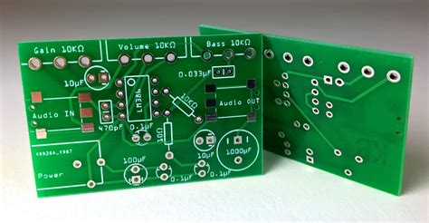
Visual inspection is the most basic and straightforward method of PCB identification. It involves examining the physical characteristics of the PCB, such as:
- Board dimensions (length, width, thickness)
- Number of layers
- Color and material of the substrate
- Component placement and orientation
- Connectors and interfaces
- Silkscreen markings and labels
While visual inspection can provide a quick overview of the PCB, it may not always be sufficient to identify the specific model or revision of the board.
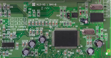
2. Part Numbers and Revision Codes
Most PCBs have part numbers and revision codes printed on the silkscreen or etched onto the board itself. These numbers are assigned by the manufacturer and can be used to identify the specific model and version of the PCB. Part numbers usually follow a specific format, which may include:
- Manufacturer prefix or logo
- Model or family designation
- Variant or option codes
- Revision or version number
For example, a part number such as “ABC-1234-567 Rev. 2” would indicate a PCB manufactured by ABC company, model 1234, variant 567, and revision 2.
3. Barcode and QR Code Scanning
Some PCBs may have barcodes or QR codes printed on the silkscreen or attached as labels. These codes can be scanned using a barcode reader or smartphone app to quickly retrieve information about the PCB, such as:
- Manufacturer and model number
- Serial number and production date
- Bill of Materials (BOM) and component list
- Assembly instructions and schematics
Barcode and QR code scanning can streamline the identification process and reduce the risk of human error.
4. Electronic Identification (ID) Chips
More advanced PCBs may incorporate electronic identification chips, such as I2C or SPI EEPROMs, which store information about the board. These chips can be accessed using a suitable programmer or microcontroller to read out the stored data, which may include:
- Manufacturer and model number
- Hardware and firmware revision
- Calibration data and settings
- Usage and maintenance logs
Electronic ID chips provide a more secure and reliable method of PCB identification, as they are less susceptible to physical damage or tampering compared to silkscreen markings or labels.
PCB Characteristics for Identification
In addition to the identification methods mentioned above, there are several key characteristics that can help identify a PCB:
1. Form Factor and Dimensions
PCBs come in various standard form factors, such as:
- ATX (Advanced Technology eXtended)
- ITX (Information Technology eXtended)
- Pico-ITX
- Nano-ITX
- Micro-ATX
- Mini-ITX
Each form factor has specific dimensions and mounting hole locations, which can be used to identify the PCB. The following table lists the dimensions of some common form factors:
| Form Factor | Width (mm) | Depth (mm) | Mounting Holes |
|---|---|---|---|
| ATX | 305 | 244 | 9 |
| Micro-ATX | 244 | 244 | 6 |
| Mini-ITX | 170 | 170 | 4 |
| Nano-ITX | 120 | 120 | 4 |
| Pico-ITX | 100 | 72 | 4 |
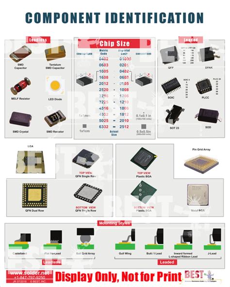
2. Number of Layers
PCBs can have different numbers of layers, depending on the complexity and density of the circuit. The most common layer configurations are:
- Single-sided (1 layer)
- Double-sided (2 layers)
- Multi-layer (4, 6, 8, or more layers)
The number of layers can be determined by examining the edge of the PCB, where the copper layers are visible as thin lines. Multi-layer boards will have additional insulating layers between the copper layers.
3. Substrate Material
The substrate material of a PCB can affect its mechanical and electrical properties, as well as its cost and manufacturability. Common substrate materials include:
- FR-4 (Flame Retardant 4)
- Rogers
- Polyimide
- Alumina
- Ceramic
The substrate material can often be identified by its color and texture. For example, FR-4 is typically green or yellow, while Rogers materials are often white or tan.
4. Component Placement and Orientation
The placement and orientation of components on a PCB can provide clues about its functionality and design. Some key factors to consider include:
- Component density and spacing
- Presence of heat sinks or cooling features
- Connector types and locations
- Power supply and voltage regulator placement
- Analog and digital circuit separation
By analyzing the component layout, an experienced engineer or technician can often deduce the intended application and performance characteristics of the PCB.

FAQ
1. What is a PCB, and why is identification important?
A: A PCB (Printed Circuit Board) is a platform that mechanically supports and electrically connects electronic components using conductive tracks, pads, and other features etched from copper sheets laminated onto a non-conductive substrate. PCB identification is important for several reasons:
- Ensuring compatibility with other components and systems
- Facilitating maintenance, repair, and troubleshooting
- Tracking product revisions and updates
- Complying with regulatory and quality control requirements
2. What are the most common methods of PCB identification?
A: The most common methods of PCB identification include:
- Visual inspection of physical characteristics and markings
- Part numbers and revision codes printed on the silkscreen or etched onto the board
- Barcode and QR code scanning for quick information retrieval
- Electronic identification chips that store board data
Each method has its own advantages and limitations, and a combination of methods may be used for more reliable identification.
3. What are some key characteristics that can help identify a PCB?
A: Some key characteristics that can help identify a PCB include:
- Form factor and dimensions, such as ATX, ITX, or custom sizes
- Number of layers, ranging from single-sided to multi-layer boards
- Substrate material, such as FR-4, Rogers, or ceramic
- Component placement and orientation, indicating functionality and design
By examining these characteristics, an experienced engineer or technician can often deduce important information about the PCB’s intended application and performance.
4. Can PCB identification be automated?
A: Yes, PCB identification can be automated to some extent using various technologies, such as:
- Machine vision systems that can analyze physical characteristics and markings
- Barcode and QR code scanners that can quickly retrieve board information
- Electronic identification chips that can be read out using suitable programmers or microcontrollers
- RFID (Radio-Frequency Identification) tags that can store and transmit board data wirelessly
Automated PCB identification can help streamline the manufacturing and maintenance processes, reduce human error, and improve traceability and quality control.
5. What should I do if I cannot identify a PCB?
A: If you cannot identify a PCB using the methods and characteristics described in this article, you may need to consult additional resources or expertise, such as:
- The manufacturer’s website or technical support
- Online forums or communities dedicated to electronics and PCB design
- Professional PCB design and manufacturing services
- Reverse engineering techniques, such as X-ray imaging or layer-by-layer analysis
In some cases, it may not be possible or practical to fully identify a PCB, especially if it is a custom or proprietary design. In such situations, it is important to document as much information as possible and seek guidance from experts in the field.
Conclusion
PCB identification is a crucial skill for anyone involved in electronics design, manufacturing, or maintenance. By understanding the various methods and characteristics used to identify PCBs, you can ensure compatibility, functionality, and maintainability of electronic systems. Visual inspection, part numbers, barcodes, and electronic ID chips are among the most common methods of PCB identification, each with its own strengths and weaknesses. Key characteristics, such as form factor, number of layers, substrate material, and component placement, can also provide valuable clues about a PCB’s intended application and performance. With the increasing complexity and miniaturization of electronic devices, automated identification technologies, such as machine vision and RFID, are becoming more important for streamlining the PCB identification process. By staying up-to-date with the latest techniques and best practices, you can master the art of PCB identification and take your electronics skills to the next level.


Leave a Reply